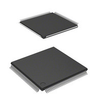
DF2161BVTE10 Renesas Electronics America, DF2161BVTE10 Datasheet - Page 45

DF2161BVTE10
Manufacturer Part Number
DF2161BVTE10
Description
MCU 3V 128K 144-TQFP
Manufacturer
Renesas Electronics America
Series
H8® H8S/2100r
Datasheet
1.DF2160BVT10V.pdf
(847 pages)
Specifications of DF2161BVTE10
Core Processor
H8S/2000
Core Size
16-Bit
Speed
10MHz
Connectivity
Host Interface (LPC), I²C, IrDA, SCI, X-Bus
Peripherals
PWM, WDT
Number Of I /o
114
Program Memory Size
128KB (128K x 8)
Program Memory Type
FLASH
Ram Size
4K x 8
Voltage - Supply (vcc/vdd)
2.7 V ~ 3.6 V
Data Converters
A/D 8x10b; D/A 2x8b
Oscillator Type
Internal
Operating Temperature
-20°C ~ 75°C
Package / Case
144-TQFP, 144-VQFP
Lead Free Status / RoHS Status
Contains lead / RoHS non-compliant
Eeprom Size
-
Other names
HD64F2161BVTE10
HD64F2161BVTE10
HD64F2161BVTE10
- Current page: 45 of 847
- Download datasheet (5Mb)
Figure 15.27 Sample Flowchart for Mode Transition during Reception................................... 410
Figure 15.28 Switching from SCK Pins to Port Pins ................................................................ 411
Figure 15.29 Prevention of Low Pulse Output at Switching from SCK Pins to Port Pins ........ 411
Section 16 I
Figure 16.1
Figure 16.2
Figure 16.3
Figure 16.4
Figure 16.5
Figure 16.6
Figure 16.7
Figure 16.8
Figure 16.9
Figure 16.10 Example of Stop Condition Issuance Operation Timing in Master Transmit
Figure 16.11 Sample Flowchart for Operations in Master Receive Mode (HNDS = 1) ........... 449
Figure 16.12 Example of Operation Timing in Master Receive Mode
Figure 16.13 Example of Stop Condition Issuance Operation Timing in Master Receive
Figure 16.14 Sample Flowchart for Operations in Master Receive Mode
Figure 16.15 Sample Flowchart for Operations in Master Receive Mode
Figure 16.16 Example of Master Receive Mode Operation Timing
Figure 16.17 Example of Stop Condition Issuance Timing in Master Receive Mode
Figure 16.18 Sample Flowchart for Operations in Slave Receive Mode (HNDS = 1).............. 458
Figure 16.19 Example of Slave Receive Mode Operation Timing (1) (MLS = 0, HNDS= 1).. 460
Figure 16.20 Example of Slave Receive Mode Operation Timing (2) (MLS = 0, HNDS= 1).. 461
Figure 16.21 Sample Flowchart for Operations in Slave Receive Mode (HNDS = 0).............. 462
Figure 16.22 Example of Slave Receive Mode Operation Timing (1)
Figure 16.23 Example of Slave Receive Mode Operation Timing (2)
Figure 16.24 Sample Flowchart for Slave Transmit Mode ....................................................... 465
Figure 16.25 Example of Slave Transmit Mode Operation Timing (MLS = 0) ........................ 467
Figure 16.26 IRIC Setting Timing and SCL Control (1)........................................................... 468
Figure 16.27 IRIC Setting Timing and SCL Control (2)........................................................... 469
2
C Bus Interface (IIC) (Optional)
Block Diagram of I
I
I
I
I
I
Sample Flowchart for IIC Initialization ............................................................... 444
Sample Flowchart for Operations in Master Transmit Mode............................... 445
Example of Operation Timing in Master Transmit Mode (MLS = WAIT = 0) ... 447
Mode (MLS = WAIT = 0) ................................................................................... 448
(MLS = WAIT = 0, HNDS = 1)........................................................................... 451
Mode (MLS = WAIT = 0, HNDS = 1) ................................................................ 451
(Receiving Multiple Bytes) (WAIT = 1).............................................................. 452
(Receiving a Single Byte) (WAIT = 1) ................................................................ 453
(MLS = ACKB = 0, WAIT = 1) .......................................................................... 456
(MLS = ACKB = 0, WAIT = 1) .......................................................................... 456
(MLS = ACKB = 0, HNDS = 0) .......................................................................... 464
(MLS = ACKB = 0, HNDS = 0) .......................................................................... 464
2
2
2
2
2
C Bus Interface Connections (Example: This LSI as Master) ........................... 416
C Bus Data Format (I
C Bus Data Format (Formatless) (IIC_0 Only) ................................................. 442
C Bus Data Format (Serial Format)................................................................... 443
C Bus Timing .................................................................................................... 443
2
C Bus Interface .................................................................... 415
2
C Bus Format) ................................................................ 442
Rev. 3.00 Mar 21, 2006 page xliii of liv
Related parts for DF2161BVTE10
Image
Part Number
Description
Manufacturer
Datasheet
Request
R

Part Number:
Description:
KIT STARTER FOR M16C/29
Manufacturer:
Renesas Electronics America
Datasheet:

Part Number:
Description:
KIT STARTER FOR R8C/2D
Manufacturer:
Renesas Electronics America
Datasheet:

Part Number:
Description:
R0K33062P STARTER KIT
Manufacturer:
Renesas Electronics America
Datasheet:

Part Number:
Description:
KIT STARTER FOR R8C/23 E8A
Manufacturer:
Renesas Electronics America
Datasheet:

Part Number:
Description:
KIT STARTER FOR R8C/25
Manufacturer:
Renesas Electronics America
Datasheet:

Part Number:
Description:
KIT STARTER H8S2456 SHARPE DSPLY
Manufacturer:
Renesas Electronics America
Datasheet:

Part Number:
Description:
KIT STARTER FOR R8C38C
Manufacturer:
Renesas Electronics America
Datasheet:

Part Number:
Description:
KIT STARTER FOR R8C35C
Manufacturer:
Renesas Electronics America
Datasheet:

Part Number:
Description:
KIT STARTER FOR R8CL3AC+LCD APPS
Manufacturer:
Renesas Electronics America
Datasheet:

Part Number:
Description:
KIT STARTER FOR RX610
Manufacturer:
Renesas Electronics America
Datasheet:

Part Number:
Description:
KIT STARTER FOR R32C/118
Manufacturer:
Renesas Electronics America
Datasheet:

Part Number:
Description:
KIT DEV RSK-R8C/26-29
Manufacturer:
Renesas Electronics America
Datasheet:

Part Number:
Description:
KIT STARTER FOR SH7124
Manufacturer:
Renesas Electronics America
Datasheet:

Part Number:
Description:
KIT STARTER FOR H8SX/1622
Manufacturer:
Renesas Electronics America
Datasheet:

Part Number:
Description:
KIT DEV FOR SH7203
Manufacturer:
Renesas Electronics America
Datasheet:


