DF2367VF33V Renesas Electronics America, DF2367VF33V Datasheet - Page 284
DF2367VF33V
Manufacturer Part Number
DF2367VF33V
Description
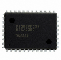
IC H8S/2367 MCU FLASH 128QFP
Manufacturer
Renesas Electronics America
Series
H8® H8S/2300r
Datasheets
1.HEWH8E10A.pdf
(19 pages)
2.D12312SVTE25V.pdf
(341 pages)
3.DF2368VTE34V.pdf
(1044 pages)
Specifications of DF2367VF33V
Core Processor
H8S/2000
Core Size
16-Bit
Speed
33MHz
Connectivity
I²C, IrDA, SCI, SmartCard
Peripherals
DMA, POR, PWM, WDT
Number Of I /o
84
Program Memory Size
384KB (384K x 8)
Program Memory Type
FLASH
Ram Size
24K x 8
Voltage - Supply (vcc/vdd)
3 V ~ 3.6 V
Data Converters
A/D 10x10b, D/A 2x8b
Oscillator Type
Internal
Operating Temperature
-20°C ~ 75°C
Package / Case
128-QFP
For Use With
YR0K42378FC000BA - KIT EVAL FOR H8S/2378HS0005KCU11H - EMULATOR E10A-USB H8S(X),SH2(A)
Lead Free Status / RoHS Status
Lead free / RoHS Compliant
Eeprom Size
-
Available stocks
Company
Part Number
Manufacturer
Quantity
Price
Company:

Part Number:
DF2367VF33V
Manufacturer:
Renesas Electronics America
Quantity:
135
Company:
Part Number:
DF2367VF33V
Manufacturer:
Renesas Electronics America
Quantity:
10 000


Section 7 DMA Controller (DMAC)
Legend:
×: Don't care
• DMACR_0B and DMACR_1B
Rev.6.00 Mar. 18, 2009 Page 224 of 980
REJ09B0050-0600
Bit
10
to
8
Bit
7
6
5
4
3
2
1
0
Bit Name
⎯
Bit Name
⎯
DAID
DAIDE
—
DTF3
DTF2
DTF1
DTF0
Initial Value
All 0
Initial Value
0
0
0
0
0
0
0
0
R/W
R/W
R/W
R/W
R/W
R/W
R/W
R/W
R/W
R/W
R/W
Reserved
Reserved
Reserved
Description
Though these bits can be read from or written to,
the write value should always be 0.
Description
Though this bit can be read from or written to,
the write value should always be 0.
Destination Address Increment/Decrement
Destination Address Increment/Decrement
Enable
These bits specify whether destination address
register MARB is to be incremented,
decremented, or left unchanged, when data
transfer is performed.
00: MARB is fixed
01: MARB is incremented after a data transfer
•
•
10: MARB is fixed
11: MARB is decremented after a data transfer
•
•
Though this bit can be read from or written to,
the write value should always be 0.
Data Transfer Factor 3 to 0
These bits select the data transfer factor
(activation source). The factors that can be
specified differ between normal mode and block
transfer mode.
When DTSZ = 0, MARB is incremented by 1
When DTSZ = 1, MARB is incremented by 2
When DTSZ = 0, MARB is decremented by 1
When DTSZ = 1, MARB is decremented by 2
Related parts for DF2367VF33V
Image
Part Number
Description
Manufacturer
Datasheet
Request
R

Part Number:
Description:
CONN PLUG 12POS DUAL 0.5MM SMD
Manufacturer:
Hirose Electric Co Ltd
Datasheet:
Part Number:
Description:
CONN PLUG 18POS DUAL 0.5MM SMD
Manufacturer:
Hirose Electric Co Ltd
Datasheet:
Part Number:
Description:
CONN PLUG 14POS DUAL 0.5MM SMD
Manufacturer:
Hirose Electric Co Ltd
Datasheet:
Part Number:
Description:
CONN RECEPT 20POS DUAL 0.5MM SMD
Manufacturer:
Hirose Electric Co Ltd
Datasheet:
Part Number:
Description:
CONN PLUG 16POS DUAL 0.5MM SMD
Manufacturer:
Hirose Electric Co Ltd
Datasheet:
Part Number:
Description:
CONN RECEPT 16POS DUAL 0.5MM SMD
Manufacturer:
Hirose Electric Co Ltd
Datasheet:
Part Number:
Description:
CONN PLUG 20POS DUAL 0.5MM SMD
Manufacturer:
Hirose Electric Co Ltd
Datasheet:
Part Number:
Description:
CONN PLUG 30POS DUAL 0.5MM SMD
Manufacturer:
Hirose Electric Co Ltd
Datasheet:
Part Number:
Description:
CONN RECEPT 30POS DUAL 0.5MM SMD
Manufacturer:
Hirose Electric Co Ltd
Datasheet:
Part Number:
Description:
CONN PLUG 40POS DUAL 0.5MM SMD
Manufacturer:
Hirose Electric Co Ltd
Datasheet:

Part Number:
Description:
KIT STARTER FOR M16C/29
Manufacturer:
Renesas Electronics America
Datasheet:

Part Number:
Description:
KIT STARTER FOR R8C/2D
Manufacturer:
Renesas Electronics America
Datasheet:

Part Number:
Description:
R0K33062P STARTER KIT
Manufacturer:
Renesas Electronics America
Datasheet:

Part Number:
Description:
KIT STARTER FOR R8C/23 E8A
Manufacturer:
Renesas Electronics America
Datasheet:

Part Number:
Description:
KIT STARTER FOR R8C/25
Manufacturer:
Renesas Electronics America
Datasheet: