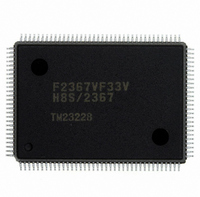
DF2367VF33V Renesas Electronics America, DF2367VF33V Datasheet - Page 417
DF2367VF33V
Manufacturer Part Number
DF2367VF33V
Description
IC H8S/2367 MCU FLASH 128QFP
Manufacturer
Renesas Electronics America
Series
H8® H8S/2300r
Datasheets
1.HEWH8E10A.pdf
(19 pages)
2.D12312SVTE25V.pdf
(341 pages)
3.DF2368VTE34V.pdf
(1044 pages)
Specifications of DF2367VF33V
Core Processor
H8S/2000
Core Size
16-Bit
Speed
33MHz
Connectivity
I²C, IrDA, SCI, SmartCard
Peripherals
DMA, POR, PWM, WDT
Number Of I /o
84
Program Memory Size
384KB (384K x 8)
Program Memory Type
FLASH
Ram Size
24K x 8
Voltage - Supply (vcc/vdd)
3 V ~ 3.6 V
Data Converters
A/D 10x10b, D/A 2x8b
Oscillator Type
Internal
Operating Temperature
-20°C ~ 75°C
Package / Case
128-QFP
For Use With
YR0K42378FC000BA - KIT EVAL FOR H8S/2378HS0005KCU11H - EMULATOR E10A-USB H8S(X),SH2(A)
Lead Free Status / RoHS Status
Lead free / RoHS Compliant
Eeprom Size
-
Available stocks
Company
Part Number
Manufacturer
Quantity
Price
Company:

Part Number:
DF2367VF33V
Manufacturer:
Renesas Electronics America
Quantity:
135
Company:
Part Number:
DF2367VF33V
Manufacturer:
Renesas Electronics America
Quantity:
10 000


9.5
Port 5 is a 4-bit I/O port. The port 5 has the following registers.
• Port 5 data direction register (P5DDR)
• Port 5 data register (P5DR)
• Port 5 register (PORT5)
9.5.1
The individual bits of P5DDR specify input or output for the pins of port 5.
P5DDR cannot be read; if it is, an undefined value will be read.
9.5.2
P5DR stores output data for the port 5 pins.
Bit
7
to
4
3
2
1
0
Bit
7
to
4
3
2
1
0
Bit Name
—
P53DDR
P52DDR
P51DDR
P50DDR
Bit Name
—
P53DR
P52DR
P51DR
P50DR
Port 5
Port 5 Data Direction Register (P5DDR)
Port 5 Data Register (P5DR)
Initial Value
All 0
0
0
0
0
Initial Value
All 0
0
0
0
0
R/W
—
W
W
W
W
R/W
—
R/W
R/W
R/W
R/W
Description
Reserved
These bits are always read as 0 and cannot be
modified.
When a pin function is specified to a general
purpose I/O, setting this bit to 1 makes the
corresponding port 1 pin an output pin, while
clearing this bit to 0 makes the pin an input pin.
Description
Reserved
These bits are always read as 0 and cannot be
modified.
Output data for a pin is stored when the pin function
is specified to a general purpose I/O.
Rev.6.00 Mar. 18, 2009 Page 357 of 980
Section 9 I/O Ports
REJ09B0050-0600
Related parts for DF2367VF33V
Image
Part Number
Description
Manufacturer
Datasheet
Request
R

Part Number:
Description:
CONN PLUG 12POS DUAL 0.5MM SMD
Manufacturer:
Hirose Electric Co Ltd
Datasheet:
Part Number:
Description:
CONN PLUG 18POS DUAL 0.5MM SMD
Manufacturer:
Hirose Electric Co Ltd
Datasheet:
Part Number:
Description:
CONN PLUG 14POS DUAL 0.5MM SMD
Manufacturer:
Hirose Electric Co Ltd
Datasheet:
Part Number:
Description:
CONN RECEPT 20POS DUAL 0.5MM SMD
Manufacturer:
Hirose Electric Co Ltd
Datasheet:
Part Number:
Description:
CONN PLUG 16POS DUAL 0.5MM SMD
Manufacturer:
Hirose Electric Co Ltd
Datasheet:
Part Number:
Description:
CONN RECEPT 16POS DUAL 0.5MM SMD
Manufacturer:
Hirose Electric Co Ltd
Datasheet:
Part Number:
Description:
CONN PLUG 20POS DUAL 0.5MM SMD
Manufacturer:
Hirose Electric Co Ltd
Datasheet:
Part Number:
Description:
CONN PLUG 30POS DUAL 0.5MM SMD
Manufacturer:
Hirose Electric Co Ltd
Datasheet:
Part Number:
Description:
CONN RECEPT 30POS DUAL 0.5MM SMD
Manufacturer:
Hirose Electric Co Ltd
Datasheet:
Part Number:
Description:
CONN PLUG 40POS DUAL 0.5MM SMD
Manufacturer:
Hirose Electric Co Ltd
Datasheet:

Part Number:
Description:
KIT STARTER FOR M16C/29
Manufacturer:
Renesas Electronics America
Datasheet:

Part Number:
Description:
KIT STARTER FOR R8C/2D
Manufacturer:
Renesas Electronics America
Datasheet:

Part Number:
Description:
R0K33062P STARTER KIT
Manufacturer:
Renesas Electronics America
Datasheet:

Part Number:
Description:
KIT STARTER FOR R8C/23 E8A
Manufacturer:
Renesas Electronics America
Datasheet:

Part Number:
Description:
KIT STARTER FOR R8C/25
Manufacturer:
Renesas Electronics America
Datasheet: