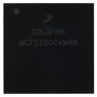
MCF5280CVM66 Freescale Semiconductor, MCF5280CVM66 Datasheet - Page 130

MCF5280CVM66
Manufacturer Part Number
MCF5280CVM66
Description
IC MPU 32BIT COLDF 256-MAPBGA
Manufacturer
Freescale Semiconductor
Series
MCF528xr
Datasheet
1.MCF5216CVM66J.pdf
(766 pages)
Specifications of MCF5280CVM66
Core Processor
Coldfire V2
Core Size
32-Bit
Speed
66MHz
Connectivity
CAN, EBI/EMI, Ethernet, I²C, SPI, UART/USART
Peripherals
DMA, LVD, POR, PWM, WDT
Number Of I /o
142
Program Memory Type
ROMless
Ram Size
64K x 8
Voltage - Supply (vcc/vdd)
2.7 V ~ 3.6 V
Data Converters
A/D 8x10b
Oscillator Type
External
Operating Temperature
-40°C ~ 85°C
Package / Case
256-MAPBGA
Controller Family/series
ColdFire
No. Of I/o's
150
Program Memory Size
2KB
Ram Memory Size
64KB
Cpu Speed
66.67MHz
Embedded Interface Type
CAN, I2C, SPI, UART
No. Of Pwm Channels
8
Rohs Compliant
Yes
Lead Free Status / RoHS Status
Lead free / RoHS Compliant
Eeprom Size
-
Program Memory Size
-
Available stocks
Company
Part Number
Manufacturer
Quantity
Price
Company:
Part Number:
MCF5280CVM66
Manufacturer:
FREESCAL
Quantity:
151
Company:
Part Number:
MCF5280CVM66
Manufacturer:
Freescale Semiconductor
Quantity:
10 000
Company:
Part Number:
MCF5280CVM66J
Manufacturer:
Freescale Semiconductor
Quantity:
10 000
Company:
Part Number:
MCF5280CVM66L
Manufacturer:
FREESCAL
Quantity:
151
- Current page: 130 of 766
- Download datasheet (9Mb)
ColdFire Flash Module (CFM)
Consider the following example for f
So, for f
for the timing of program and erase operations.
When CFMCLKD is written, the DIVLD bit is set automatically. If DIVLD is 0, CFMCLKD has not been
written since the last reset. Program and erase commands will not execute if this register has not been
written (see
6.4.3.2
A command state machine is used to supervise the write sequencing of program, erase, and verify
commands. To prepare for a command, the CFMUSTAT[CBEIF] flag should be tested to ensure that the
address, data, and command buffers are empty. If CBEIF is set, the command write sequence can be
started.
This three-step command write sequence must be strictly followed. No intermediate writes to the CFM
module are permitted between these three steps. The command write sequence is:
6-18
1. Write the 32-bit longword to be programmed to its location in the CFM array. The address and data
will be stored in internal buffers. All address bits are valid for program commands. The value of
the data written for verify and erase commands is ignored. For mass erase or verify, the address can
be any location in the CFM array. For page erase, address bits [9:0] are ignored.
SYS
= 66 MHz, writing 0x54 to CFMCLKD will set f
Section 6.4.3.4, “Flash User Mode Illegal
Program, Erase, and Verify Sequences
For proper program and erase operations, it is critical to set f
150 kHz and 200 kHz. Array damage due to overstress can occur when f
is less than 150 kHz. Incomplete programming and erasure can occur when
f
Command execution time increases proportionally with the period of f
CLK
is greater than 200 kHz.
MCF5282 and MCF5216 ColdFire Microcontroller User’s Manual, Rev. 3
f
CLK
DIV[5:0] =
f
CLK
=
=
SYS
=
=
2 x (DIV[5:0] + 1) x (1 + (PRDIV8 x 7))
= 66 MHz:
2 x (DIV[5:0] + 1) x (1 + (PRDIV8 x 7))
2 x 200kHz x (1 + (PRDIV8 x 7))
2 x (20 + 1) x (1 + (1 x 7))
400 kHz x (1 + (1 x 7))
WARNING
NOTE
66 MHz
66 MHz
Operations”).
f
f
SYS
SYS
f
SYS
CLK
to 196.43 kHz which is a valid frequency
= 196.43 kHz
= 20
CLK
between
Freescale Semiconductor
CLK
CLK
.
Related parts for MCF5280CVM66
Image
Part Number
Description
Manufacturer
Datasheet
Request
R
Part Number:
Description:
Manufacturer:
Freescale Semiconductor, Inc
Datasheet:
Part Number:
Description:
Manufacturer:
Freescale Semiconductor, Inc
Datasheet:
Part Number:
Description:
Manufacturer:
Freescale Semiconductor, Inc
Datasheet:
Part Number:
Description:
Manufacturer:
Freescale Semiconductor, Inc
Datasheet:
Part Number:
Description:
Manufacturer:
Freescale Semiconductor, Inc
Datasheet:
Part Number:
Description:
Manufacturer:
Freescale Semiconductor, Inc
Datasheet:
Part Number:
Description:
Manufacturer:
Freescale Semiconductor, Inc
Datasheet:
Part Number:
Description:
Manufacturer:
Freescale Semiconductor, Inc
Datasheet:
Part Number:
Description:
Manufacturer:
Freescale Semiconductor, Inc
Datasheet:
Part Number:
Description:
Manufacturer:
Freescale Semiconductor, Inc
Datasheet:
Part Number:
Description:
Manufacturer:
Freescale Semiconductor, Inc
Datasheet:
Part Number:
Description:
Manufacturer:
Freescale Semiconductor, Inc
Datasheet:
Part Number:
Description:
Manufacturer:
Freescale Semiconductor, Inc
Datasheet:
Part Number:
Description:
Manufacturer:
Freescale Semiconductor, Inc
Datasheet:
Part Number:
Description:
Manufacturer:
Freescale Semiconductor, Inc
Datasheet:


