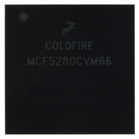
MCF5280CVM66 Freescale Semiconductor, MCF5280CVM66 Datasheet - Page 309

MCF5280CVM66
Manufacturer Part Number
MCF5280CVM66
Description
IC MPU 32BIT COLDF 256-MAPBGA
Manufacturer
Freescale Semiconductor
Series
MCF528xr
Datasheet
1.MCF5216CVM66J.pdf
(766 pages)
Specifications of MCF5280CVM66
Core Processor
Coldfire V2
Core Size
32-Bit
Speed
66MHz
Connectivity
CAN, EBI/EMI, Ethernet, I²C, SPI, UART/USART
Peripherals
DMA, LVD, POR, PWM, WDT
Number Of I /o
142
Program Memory Type
ROMless
Ram Size
64K x 8
Voltage - Supply (vcc/vdd)
2.7 V ~ 3.6 V
Data Converters
A/D 8x10b
Oscillator Type
External
Operating Temperature
-40°C ~ 85°C
Package / Case
256-MAPBGA
Controller Family/series
ColdFire
No. Of I/o's
150
Program Memory Size
2KB
Ram Memory Size
64KB
Cpu Speed
66.67MHz
Embedded Interface Type
CAN, I2C, SPI, UART
No. Of Pwm Channels
8
Rohs Compliant
Yes
Lead Free Status / RoHS Status
Lead free / RoHS Compliant
Eeprom Size
-
Program Memory Size
-
Available stocks
Company
Part Number
Manufacturer
Quantity
Price
Company:
Part Number:
MCF5280CVM66
Manufacturer:
FREESCAL
Quantity:
151
Company:
Part Number:
MCF5280CVM66
Manufacturer:
Freescale Semiconductor
Quantity:
10 000
Company:
Part Number:
MCF5280CVM66J
Manufacturer:
Freescale Semiconductor
Quantity:
10 000
Company:
Part Number:
MCF5280CVM66L
Manufacturer:
FREESCAL
Quantity:
151
- Current page: 309 of 766
- Download datasheet (9Mb)
peripheral device or memory, the source address is the starting address of the data block. This can be any
aligned byte address.
The DARn should contain the destination (write) address. If the transfer is from a peripheral device to
memory, or from memory to memory, the DARn is loaded with the starting address of the data block to be
written. If the transfer is from memory to a peripheral device, DARn is loaded with the address of the
peripheral data register. This address can be any aligned byte address.
SARn and DARn change after each cycle depending on DCRn[SSIZE,DSIZE, SINC,DINC] and on the
starting address. Increment values can be 1, 2, 4, or 16 for byte, word, longword, or 16-byte line transfers,
respectively. If the address register is programmed to remain unchanged (no count), the register is not
incremented after the data transfer.
BCRn[BCR] must be loaded with the number of byte transfers to occur. It is decremented by 1, 2, 4, or 16
at the end of each transfer, depending on the transfer size. DSRn[DONE] must be cleared for channel
startup.
As soon as the channel has been initialized, it is started by writing a one to DCRn[START] or asserting
DREQn, depending on the status of DCRn[EEXT]. Programming the channel for internal requests causes
the channel to request the bus and start transferring data immediately. If the channel is programmed for
external request, DREQn must be asserted before the channel requests the bus.
Changes to DCRn are effective immediately while the channel is active. To avoid problems with changing
a DMA channel setup, write a one to DSRn[DONE] to stop the DMA channel.
16.5.4
This section describes auto-alignment and bandwidth control for DMA transfers.
16.5.4.1 Auto-Alignment
Auto-alignment allows block transfers to occur at the optimal size based on the address, byte count, and
programmed size. To use this feature, DCRn[AA] must be set. The source is auto-aligned if DCRn[SSIZE]
indicates a transfer size larger than DCRn[DSIZE]. Source alignment takes precedence over the
destination when the source and destination sizes are equal. Otherwise, the destination is auto-aligned. The
address register chosen for alignment increments regardless of the increment value. Configuration error
checking is performed on registers not chosen for alignment.
If BCRn is greater than 16, the address determines transfer size. Bytes, words, or longwords are transferred
until the address is aligned to the programmed size boundary, at which time accesses begin using the
programmed size.
If BCRn is less than 16 at the start of a transfer, the number of bytes remaining dictates transfer size. For
example, AA = 1, SARn = 0x0001, BCRn = 0x00F0, SSIZE = 00 (longword), and DSIZE = 01 (byte).
Because SSIZE > DSIZE, the source is auto-aligned. Error checking is performed on destination registers.
The access sequence is as follows:
Freescale Semiconductor
1. Read byte from 0x0001—write 1 byte, increment SARn.
2. Read word from 0x0002—write 2 bytes, increment SARn.
3. Read longword from 0x0004—write 4 bytes, increment SARn.
4. Repeat longwords until SARn = 0x00F0.
5. Read byte from 0x00F0—write byte, increment SARn.
Data Transfer
MCF5282 and MCF5216 ColdFire Microcontroller User’s Manual, Rev. 3
DMA Controller Module
16-13
Related parts for MCF5280CVM66
Image
Part Number
Description
Manufacturer
Datasheet
Request
R
Part Number:
Description:
Manufacturer:
Freescale Semiconductor, Inc
Datasheet:
Part Number:
Description:
Manufacturer:
Freescale Semiconductor, Inc
Datasheet:
Part Number:
Description:
Manufacturer:
Freescale Semiconductor, Inc
Datasheet:
Part Number:
Description:
Manufacturer:
Freescale Semiconductor, Inc
Datasheet:
Part Number:
Description:
Manufacturer:
Freescale Semiconductor, Inc
Datasheet:
Part Number:
Description:
Manufacturer:
Freescale Semiconductor, Inc
Datasheet:
Part Number:
Description:
Manufacturer:
Freescale Semiconductor, Inc
Datasheet:
Part Number:
Description:
Manufacturer:
Freescale Semiconductor, Inc
Datasheet:
Part Number:
Description:
Manufacturer:
Freescale Semiconductor, Inc
Datasheet:
Part Number:
Description:
Manufacturer:
Freescale Semiconductor, Inc
Datasheet:
Part Number:
Description:
Manufacturer:
Freescale Semiconductor, Inc
Datasheet:
Part Number:
Description:
Manufacturer:
Freescale Semiconductor, Inc
Datasheet:
Part Number:
Description:
Manufacturer:
Freescale Semiconductor, Inc
Datasheet:
Part Number:
Description:
Manufacturer:
Freescale Semiconductor, Inc
Datasheet:
Part Number:
Description:
Manufacturer:
Freescale Semiconductor, Inc
Datasheet:


