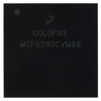
MCF5280CVM66 Freescale Semiconductor, MCF5280CVM66 Datasheet - Page 273

MCF5280CVM66
Manufacturer Part Number
MCF5280CVM66
Description
IC MPU 32BIT COLDF 256-MAPBGA
Manufacturer
Freescale Semiconductor
Series
MCF528xr
Datasheet
1.MCF5216CVM66J.pdf
(766 pages)
Specifications of MCF5280CVM66
Core Processor
Coldfire V2
Core Size
32-Bit
Speed
66MHz
Connectivity
CAN, EBI/EMI, Ethernet, I²C, SPI, UART/USART
Peripherals
DMA, LVD, POR, PWM, WDT
Number Of I /o
142
Program Memory Type
ROMless
Ram Size
64K x 8
Voltage - Supply (vcc/vdd)
2.7 V ~ 3.6 V
Data Converters
A/D 8x10b
Oscillator Type
External
Operating Temperature
-40°C ~ 85°C
Package / Case
256-MAPBGA
Controller Family/series
ColdFire
No. Of I/o's
150
Program Memory Size
2KB
Ram Memory Size
64KB
Cpu Speed
66.67MHz
Embedded Interface Type
CAN, I2C, SPI, UART
No. Of Pwm Channels
8
Rohs Compliant
Yes
Lead Free Status / RoHS Status
Lead free / RoHS Compliant
Eeprom Size
-
Program Memory Size
-
Available stocks
Company
Part Number
Manufacturer
Quantity
Price
Company:
Part Number:
MCF5280CVM66
Manufacturer:
FREESCAL
Quantity:
151
Company:
Part Number:
MCF5280CVM66
Manufacturer:
Freescale Semiconductor
Quantity:
10 000
Company:
Part Number:
MCF5280CVM66J
Manufacturer:
Freescale Semiconductor
Quantity:
10 000
Company:
Part Number:
MCF5280CVM66L
Manufacturer:
FREESCAL
Quantity:
151
- Current page: 273 of 766
- Download datasheet (9Mb)
Chapter 15
Synchronous DRAM Controller Module
This chapter describes configuration and operation of the synchronous DRAM (SDRAM) controller. It
begins with a general description and brief glossary, and includes a description of signals involved in
DRAM operations. The remainder of the chapter describes the programming model and signal timing, as
well as the command set required for synchronous operations. It also includes extensive examples that the
designer can follow to better understand how to configure the DRAM controller for synchronous
operations.
15.1
The synchronous DRAM controller module provides glueless integration of SDRAM with the ColdFire
product. The key features of the DRAM controller include the following:
15.1.1
The following terminology is used in this chapter:
15.1.2
The basic components of the SDRAM controller are shown in
Freescale Semiconductor
•
•
•
•
•
•
•
Support for two independent blocks of SDRAM
Interface to standard SDRAM components
Programmable SRAS, SCAS, and refresh timing
Support for 8-, 16-, and 32-bit wide SDRAM blocks
SDRAM block: Any group of DRAM memories selected by one of the SRAS[1:0] signals. Thus,
the processor can support two independent memory blocks. The base address of each block is
programmed in the DRAM address and control registers (DACR0 and DACR1).
SDRAM: RAMs that operate like asynchronous DRAMs but with a synchronous clock, a
pipelined, multiple-bank architecture, and a faster speed.
SDRAM bank: An internal partition in an SDRAM device. For example, a 64-Mbit SDRAM
component might be configured as four 512K x 32 banks. Banks are selected through the SDRAM
component’s bank select lines.
Overview
Definitions
Block Diagram and Major Components
MCF5282 and MCF5216 ColdFire Microcontroller User’s Manual, Rev. 3
Figure
15-1.
15-1
Related parts for MCF5280CVM66
Image
Part Number
Description
Manufacturer
Datasheet
Request
R
Part Number:
Description:
Manufacturer:
Freescale Semiconductor, Inc
Datasheet:
Part Number:
Description:
Manufacturer:
Freescale Semiconductor, Inc
Datasheet:
Part Number:
Description:
Manufacturer:
Freescale Semiconductor, Inc
Datasheet:
Part Number:
Description:
Manufacturer:
Freescale Semiconductor, Inc
Datasheet:
Part Number:
Description:
Manufacturer:
Freescale Semiconductor, Inc
Datasheet:
Part Number:
Description:
Manufacturer:
Freescale Semiconductor, Inc
Datasheet:
Part Number:
Description:
Manufacturer:
Freescale Semiconductor, Inc
Datasheet:
Part Number:
Description:
Manufacturer:
Freescale Semiconductor, Inc
Datasheet:
Part Number:
Description:
Manufacturer:
Freescale Semiconductor, Inc
Datasheet:
Part Number:
Description:
Manufacturer:
Freescale Semiconductor, Inc
Datasheet:
Part Number:
Description:
Manufacturer:
Freescale Semiconductor, Inc
Datasheet:
Part Number:
Description:
Manufacturer:
Freescale Semiconductor, Inc
Datasheet:
Part Number:
Description:
Manufacturer:
Freescale Semiconductor, Inc
Datasheet:
Part Number:
Description:
Manufacturer:
Freescale Semiconductor, Inc
Datasheet:
Part Number:
Description:
Manufacturer:
Freescale Semiconductor, Inc
Datasheet:


