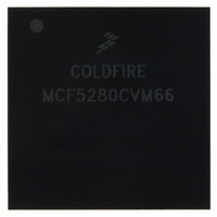
MCF5280CVM66 Freescale Semiconductor, MCF5280CVM66 Datasheet - Page 669

MCF5280CVM66
Manufacturer Part Number
MCF5280CVM66
Description
IC MPU 32BIT COLDF 256-MAPBGA
Manufacturer
Freescale Semiconductor
Series
MCF528xr
Datasheet
1.MCF5216CVM66J.pdf
(766 pages)
Specifications of MCF5280CVM66
Core Processor
Coldfire V2
Core Size
32-Bit
Speed
66MHz
Connectivity
CAN, EBI/EMI, Ethernet, I²C, SPI, UART/USART
Peripherals
DMA, LVD, POR, PWM, WDT
Number Of I /o
142
Program Memory Type
ROMless
Ram Size
64K x 8
Voltage - Supply (vcc/vdd)
2.7 V ~ 3.6 V
Data Converters
A/D 8x10b
Oscillator Type
External
Operating Temperature
-40°C ~ 85°C
Package / Case
256-MAPBGA
Controller Family/series
ColdFire
No. Of I/o's
150
Program Memory Size
2KB
Ram Memory Size
64KB
Cpu Speed
66.67MHz
Embedded Interface Type
CAN, I2C, SPI, UART
No. Of Pwm Channels
8
Rohs Compliant
Yes
Lead Free Status / RoHS Status
Lead free / RoHS Compliant
Eeprom Size
-
Program Memory Size
-
Available stocks
Company
Part Number
Manufacturer
Quantity
Price
Company:
Part Number:
MCF5280CVM66
Manufacturer:
FREESCAL
Quantity:
151
Company:
Part Number:
MCF5280CVM66
Manufacturer:
Freescale Semiconductor
Quantity:
10 000
Company:
Part Number:
MCF5280CVM66J
Manufacturer:
Freescale Semiconductor
Quantity:
10 000
Company:
Part Number:
MCF5280CVM66L
Manufacturer:
FREESCAL
Quantity:
151
- Current page: 669 of 766
- Download datasheet (9Mb)
31.4.2.3 Bypass Register
The bypass register is a single-bit shift register path from TDI to TDO when the BYPASS instruction is
selected.
31.4.2.4 JTAG_CFM_CLKDIV Register
The JTAG_CFM_CLKDIV register is a 7-bit clock divider for the CFM that is used with the
LOCKOUT_RECOVERY instruction. It controls the period of the clock used for timed events in the CFM
erase algorithm. The JTAG_CFM_CLKDIV register must be loaded before the lockout sequence can
begin.
31.4.2.5 TEST_CTRL Register
The TEST_CTRL register is a 3-bit shift register path from TDI to TDO when the
ENABLE_TEST_CTRL instruction is selected. The TEST_CTRL transfers its value to a parallel hold
register on the rising edge of TCLK when the TAP state machine is in the update-DR state.
31.4.2.6 Boundary Scan Register
The boundary scan register is connected between TDI and TDO when the EXTEST or
SAMPLE/PRELOAD instruction is selected. It captures input pin data, forces fixed values on output pins,
and selects a logic value and direction for bidirectional pins or high impedance for tri-stated pins.
The boundary scan register contains bits for bonded-out and non bonded-out signals excluding JTAG
signals, analog signals, power supplies, compliance enable pins, and clock signals.
31.5
31.5.1
The JTAG module consists of a TAP controller state machine, which is responsible for generating all
control signals that execute the JTAG instructions and read/write data registers.
Freescale Semiconductor
31–28
27–22
21–12
11–1
Bits
0
Functional Description
JTAG Module
JEDEC Joint electron device engineering council ID bits. Indicate the reduced JEDEC ID for Freescale.
Name
PRN
PIN
DC
ID
Part revision number. Indicate the revision number of the project.
Design center.
Part identification number. Indicate the device number.
IDCODE register ID. This bit is set to 1 to identify the register as the IDCODE register and not the
bypass register according to the IEEE standard 1149.1.
MCF5282 and MCF5216 ColdFire Microcontroller User’s Manual, Rev. 3
Table 31-4. IDCODE Register Field Descriptions
Description
IEEE 1149.1 Test Access Port (JTAG)
31-5
Related parts for MCF5280CVM66
Image
Part Number
Description
Manufacturer
Datasheet
Request
R
Part Number:
Description:
Manufacturer:
Freescale Semiconductor, Inc
Datasheet:
Part Number:
Description:
Manufacturer:
Freescale Semiconductor, Inc
Datasheet:
Part Number:
Description:
Manufacturer:
Freescale Semiconductor, Inc
Datasheet:
Part Number:
Description:
Manufacturer:
Freescale Semiconductor, Inc
Datasheet:
Part Number:
Description:
Manufacturer:
Freescale Semiconductor, Inc
Datasheet:
Part Number:
Description:
Manufacturer:
Freescale Semiconductor, Inc
Datasheet:
Part Number:
Description:
Manufacturer:
Freescale Semiconductor, Inc
Datasheet:
Part Number:
Description:
Manufacturer:
Freescale Semiconductor, Inc
Datasheet:
Part Number:
Description:
Manufacturer:
Freescale Semiconductor, Inc
Datasheet:
Part Number:
Description:
Manufacturer:
Freescale Semiconductor, Inc
Datasheet:
Part Number:
Description:
Manufacturer:
Freescale Semiconductor, Inc
Datasheet:
Part Number:
Description:
Manufacturer:
Freescale Semiconductor, Inc
Datasheet:
Part Number:
Description:
Manufacturer:
Freescale Semiconductor, Inc
Datasheet:
Part Number:
Description:
Manufacturer:
Freescale Semiconductor, Inc
Datasheet:
Part Number:
Description:
Manufacturer:
Freescale Semiconductor, Inc
Datasheet:


