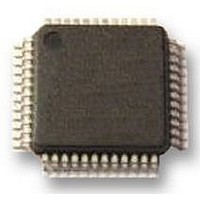
UPD78F0413GA-GAM-AX NEC, UPD78F0413GA-GAM-AX Datasheet - Page 300

UPD78F0413GA-GAM-AX
Manufacturer Part Number
UPD78F0413GA-GAM-AX
Description
8BIT UC, 32K FLASH, 1KB RAM, LCD
Manufacturer
NEC
Datasheet
1.UPD78F0413GA-GAM-AX.pdf
(562 pages)
Specifications of UPD78F0413GA-GAM-AX
Controller Family/series
UPD78F
No. Of I/o's
30
Ram Memory Size
1024Byte
Cpu Speed
10MHz
No. Of Timers
8
No. Of Pwm
RoHS Compliant
Core Size
8bit
Program Memory Size
32KB
Oscillator Type
External, Internal
Available stocks
Company
Part Number
Manufacturer
Quantity
Price
Company:
Part Number:
UPD78F0413GA-GAM-AX
Manufacturer:
ADI
Quantity:
882
Company:
Part Number:
UPD78F0413GA-GAM-AX
Manufacturer:
Renesas Electronics America
Quantity:
10 000
- Current page: 300 of 562
- Download datasheet (4Mb)
Address: FF8FH After reset: 08H R/W
300
Symbol
ADPC0
Cautions 1. Set the channel used for A/D conversion to the input mode by using port mode register 2
ADPC02
CHAPTER 12 10-BIT SUCCESSIVE APPROXIMATION TYPE A/D CONVERTER ( PD78F041x only)
7
0
2. Do not set the pin set by ADPC0 as digital I/O by ADS, ADDS1, or ADDS0.
3. If data is written to ADPC0, a wait cycle is generated. Do not write data to ADPC0 when the
4. If pins ANI0/P20/SEG21 to ANI5/P25/SEG16 are set to segment output via the PF2 register,
0
0
0
0
1
1
1
(PM2).
CPU is operating on the subsystem clock and the peripheral hardware clock is stopped. For
details, see CHAPTER 29 CAUTIONS FOR WAIT.
output is set to segment output, regardless of the ADPC0 setting.
Other than above
Figure 12-9. Format of A/D Port Configuration Register 0 (ADPC0)
ADPC01
6
0
0
0
1
1
0
0
1
ADPC00
5
0
0
1
0
1
0
1
0
User’s Manual U18698EJ1V0UD
Setting prohibited
/ANI5
P25
A
A
A
A
A
A
D
4
0
/ANI4
P24
Digital I/O (D)/analog input (A) switching
D
D
A
A
A
A
A
3
0
/ANI3
P23
D
D
D
A
A
A
A
ADPC02
2
/AN2
P22
D
D
D
D
A
A
A
ADPC01
1
/ANI1
P21
D
D
D
D
D
A
A
ADPC00
/ANI0
0
P20
D
D
D
D
D
D
A
Related parts for UPD78F0413GA-GAM-AX
Image
Part Number
Description
Manufacturer
Datasheet
Request
R

Part Number:
Description:
16/8 bit single-chip microcomputer
Manufacturer:
NEC
Datasheet:

Part Number:
Description:
Dual audio power amp circuit
Manufacturer:
NEC
Datasheet:

Part Number:
Description:
Dual comparator
Manufacturer:
NEC
Datasheet:

Part Number:
Description:
MOS type composite field effect transistor
Manufacturer:
NEC
Datasheet:

Part Number:
Description:
50 V/100 mA FET array incorporating 2 N-ch MOSFETs
Manufacturer:
NEC
Datasheet:

Part Number:
Description:
6-pin small MM high-frequency double transistor
Manufacturer:
NEC
Datasheet:

Part Number:
Description:
6-pin small MM high-frequency double transistor
Manufacturer:
NEC
Datasheet:

Part Number:
Description:
6-pin small MM high-frequency double transistor
Manufacturer:
NEC
Datasheet:

Part Number:
Description:
6-pin small MM high-frequency double transistor
Manufacturer:
NEC
Datasheet:

Part Number:
Description:
Twin transistors equipped with different model chips(6P small MM)
Manufacturer:
NEC
Datasheet:

Part Number:
Description:
Bipolar analog integrated circuit
Manufacturer:
NEC
Datasheet:


