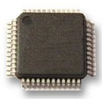
UPD78F0413GA-GAM-AX NEC, UPD78F0413GA-GAM-AX Datasheet - Page 426

UPD78F0413GA-GAM-AX
Manufacturer Part Number
UPD78F0413GA-GAM-AX
Description
8BIT UC, 32K FLASH, 1KB RAM, LCD
Manufacturer
NEC
Datasheet
1.UPD78F0413GA-GAM-AX.pdf
(562 pages)
Specifications of UPD78F0413GA-GAM-AX
Controller Family/series
UPD78F
No. Of I/o's
30
Ram Memory Size
1024Byte
Cpu Speed
10MHz
No. Of Timers
8
No. Of Pwm
RoHS Compliant
Core Size
8bit
Program Memory Size
32KB
Oscillator Type
External, Internal
Available stocks
Company
Part Number
Manufacturer
Quantity
Price
Company:
Part Number:
UPD78F0413GA-GAM-AX
Manufacturer:
ADI
Quantity:
882
Company:
Part Number:
UPD78F0413GA-GAM-AX
Manufacturer:
Renesas Electronics America
Quantity:
10 000
- Current page: 426 of 562
- Download datasheet (4Mb)
16.4.3 Bit sequential buffer mode
(1) Register description
426
Address: FF4CH
MC0CTL0
The bit sequential buffer mode is used to output sequential signals using the MCGO pin.
Symbol
The MCG control register 0 (MC0CTL0), MCG control register 1 (MC0CTL1), and MCG control register 2
(MC0CTL2) are used to set the bit sequential buffer mode.
(a) MCG control register 0 (MC0CTL0)
This register can be set by a 1-bit or 8-bit memory manipulation instruction.
Reset signal generation sets this register to 10H.
Caution Clear (0) the MC0PWR bit before rewriting the MC0DIR, MC0OSL, and MC0OLV bits (it is
MC0PWR
MC0PWR
MC0OSL
MC0OLV
MC0DIR
<7>
0
1
0
1
0
1
0
1
After reset: 10H
possible to rewrite these bits by an 8-bit memory manipulation instruction at the same
time when the MC0PWR bit is set (1)).
Operation stopped
Operation enabled
MSB
LSB
Manchester code
Bit sequential data
Low level
High level
6
0
CHAPTER 16 MANCHESTER CODE GENERATOR
R/W
5
0
User’s Manual U18698EJ1V0UD
Output level when transmission suspended
MC0DIR
<4>
First bit specification
Operation control
Data format
3
0
2
0
MC0OSL
<1>
MC0OLV
<0>
Related parts for UPD78F0413GA-GAM-AX
Image
Part Number
Description
Manufacturer
Datasheet
Request
R

Part Number:
Description:
16/8 bit single-chip microcomputer
Manufacturer:
NEC
Datasheet:

Part Number:
Description:
Dual audio power amp circuit
Manufacturer:
NEC
Datasheet:

Part Number:
Description:
Dual comparator
Manufacturer:
NEC
Datasheet:

Part Number:
Description:
MOS type composite field effect transistor
Manufacturer:
NEC
Datasheet:

Part Number:
Description:
50 V/100 mA FET array incorporating 2 N-ch MOSFETs
Manufacturer:
NEC
Datasheet:

Part Number:
Description:
6-pin small MM high-frequency double transistor
Manufacturer:
NEC
Datasheet:

Part Number:
Description:
6-pin small MM high-frequency double transistor
Manufacturer:
NEC
Datasheet:

Part Number:
Description:
6-pin small MM high-frequency double transistor
Manufacturer:
NEC
Datasheet:

Part Number:
Description:
6-pin small MM high-frequency double transistor
Manufacturer:
NEC
Datasheet:

Part Number:
Description:
Twin transistors equipped with different model chips(6P small MM)
Manufacturer:
NEC
Datasheet:

Part Number:
Description:
Bipolar analog integrated circuit
Manufacturer:
NEC
Datasheet:


