UPD78F0413GA-GAM-AX NEC, UPD78F0413GA-GAM-AX Datasheet - Page 7
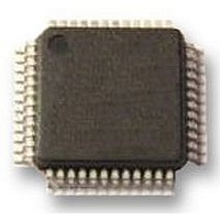
UPD78F0413GA-GAM-AX
Manufacturer Part Number
UPD78F0413GA-GAM-AX
Description
8BIT UC, 32K FLASH, 1KB RAM, LCD
Manufacturer
NEC
Datasheet
1.UPD78F0413GA-GAM-AX.pdf
(562 pages)
Specifications of UPD78F0413GA-GAM-AX
Controller Family/series
UPD78F
No. Of I/o's
30
Ram Memory Size
1024Byte
Cpu Speed
10MHz
No. Of Timers
8
No. Of Pwm
RoHS Compliant
Core Size
8bit
Program Memory Size
32KB
Oscillator Type
External, Internal
Available stocks
Company
Part Number
Manufacturer
Quantity
Price
Company:

Part Number:
UPD78F0413GA-GAM-AX
Manufacturer:
ADI
Quantity:
882
Company:
Part Number:
UPD78F0413GA-GAM-AX
Manufacturer:
Renesas Electronics America
Quantity:
10 000


CHAPTER 1 OUTLINE ............................................................................................................................ 14
CHAPTER 2 PIN FUNCTIONS ............................................................................................................... 27
CHAPTER 3 CPU ARCHITECTURE...................................................................................................... 41
1.1 Features ........................................................................................................................................ 14
1.2 Applications.................................................................................................................................. 15
1.3 Ordering Information ................................................................................................................... 15
1.4 Pin Configuration (Top View)...................................................................................................... 16
1.5 78K0/Lx3 Microcontroller Series Lineup ................................................................................... 19
1.6 Block Diagram .............................................................................................................................. 23
1.7 Outline of Functions .................................................................................................................... 24
2.1 Pin Function List .......................................................................................................................... 27
2.2 Description of Pin Functions ...................................................................................................... 31
2.3 Pin I/O Circuits and Recommended Connection of Unused Pins........................................... 37
3.1 Memory Space .............................................................................................................................. 41
3.2 Processor Registers .................................................................................................................... 54
3.3 Instruction Address Addressing ................................................................................................ 64
2.2.1 P12, P13 (port 1) .............................................................................................................................31
2.2.2 P20 to P25 (port 2)...........................................................................................................................31
2.2.3 P31 to P34 (port 3)...........................................................................................................................32
2.2.4 P40 (port 4)......................................................................................................................................33
2.2.5 P100, P101 (port 10)........................................................................................................................33
2.2.6 P112, P113 (port 11)........................................................................................................................33
2.2.7 P120 to P124 (port 12).....................................................................................................................34
2.2.8 P140 to P143 (port 14).....................................................................................................................34
2.2.9 P150 to P153 (port 15).....................................................................................................................35
2.2.10 AV
2.2.11 AV
2.2.12 COM0 to COM7 .............................................................................................................................35
2.2.13 V
2.2.14 RESET...........................................................................................................................................35
2.2.15 REGC ............................................................................................................................................36
2.2.16 V
2.2.17 V
2.2.18 FLMD0 ...........................................................................................................................................36
3.1.1 Internal program memory space ......................................................................................................47
3.1.2 Internal data memory space ............................................................................................................49
3.1.3 Special function register (SFR) area ................................................................................................49
3.1.4 Data memory addressing.................................................................................................................50
3.2.1 Control registers...............................................................................................................................54
3.2.2 General-purpose registers ...............................................................................................................58
3.2.3 Special function registers (SFRs).....................................................................................................59
LC0
DD
SS
REF
SS
.................................................................................................................................................36
.................................................................................................................................................36
to V
( PD78F041x only) ...............................................................................................................35
( PD78F041x only) ............................................................................................................35
LC3
....................................................................................................................................35
User’s Manual U18698EJ1V0UD
CONTENTS
7
Related parts for UPD78F0413GA-GAM-AX
Image
Part Number
Description
Manufacturer
Datasheet
Request
R

Part Number:
Description:
16/8 bit single-chip microcomputer
Manufacturer:
NEC
Datasheet:
Part Number:
Description:
Dual audio power amp circuit
Manufacturer:
NEC
Datasheet:
Part Number:
Description:
Dual comparator
Manufacturer:
NEC
Datasheet:
Part Number:
Description:
MOS type composite field effect transistor
Manufacturer:
NEC
Datasheet:
Part Number:
Description:
50 V/100 mA FET array incorporating 2 N-ch MOSFETs
Manufacturer:
NEC
Datasheet:
Part Number:
Description:
6-pin small MM high-frequency double transistor
Manufacturer:
NEC
Datasheet:
Part Number:
Description:
6-pin small MM high-frequency double transistor
Manufacturer:
NEC
Datasheet:
Part Number:
Description:
6-pin small MM high-frequency double transistor
Manufacturer:
NEC
Datasheet:
Part Number:
Description:
6-pin small MM high-frequency double transistor
Manufacturer:
NEC
Datasheet:
Part Number:
Description:
Twin transistors equipped with different model chips(6P small MM)
Manufacturer:
NEC
Datasheet:
Part Number:
Description:
Bipolar analog integrated circuit
Manufacturer:
NEC
Datasheet: