EVAL-ADAU1761Z Analog Devices Inc, EVAL-ADAU1761Z Datasheet - Page 26
EVAL-ADAU1761Z
Manufacturer Part Number
EVAL-ADAU1761Z
Description
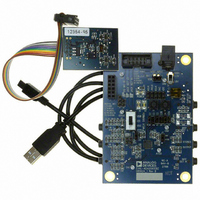
Eval Board For ADAU1761
Manufacturer
Analog Devices Inc
Series
SigmaDSP®r
Specifications of EVAL-ADAU1761Z
Main Purpose
Audio, CODEC
Embedded
Yes, DSP
Utilized Ic / Part
ADAU1761
Primary Attributes
Stereo, 24-Bit, 8 ~ 96 kHz Sampling Rate, GUI Tool
Secondary Attributes
I²C and GPIO Interfaces, 2 Differential and 1 Stereo Single-Ended Analog Inputs and Outputs
Silicon Manufacturer
Analog Devices
Core Architecture
SigmaDSP
Silicon Core Number
ADAU1761
Silicon Family Name
SigmaDSP
Application Sub Type
Audio
Lead Free Status / RoHS Status
Lead free / RoHS Compliant
Available stocks
Company
Part Number
Manufacturer
Quantity
Price
Company:

Part Number:
EVAL-ADAU1761Z
Manufacturer:
Analog Devices Inc
Quantity:
135


ADAU1761
CLOCKING AND SAMPLING RATES
CORE CLOCK
Clocks for the converters, the serial ports, and the DSP are
derived from the core clock. The core clock can be derived
directly from MCLK or it can be generated by the PLL. The
CLKSRC bit (Bit 3 in Register R0, Address 0x4000) determines
the clock source.
The INFREQ[1:0] bits should be set according to the expected
input clock rate selected by CLKSRC; this value also determines
the core clock rate and the base sampling frequency, f
For example, if the input to CLKSRC = 49.152 MHz (from
PLL), then
The PLL output clock rate is always 1024 × f
control register automatically sets the INFREQ[1:0] bits to
1024 × f
INFREQ[1:0] frequency should be set according to the MCLK
pin clock rate and the desired base sampling frequency.
INFREQ[1:0] = 1024 × f
f
S
= 49.152 MHz/1024 = 48 kHz
S
when using the PLL. When using a direct clock, the
MCLK
R1: PLL CONTROL REGISTER
÷ X
S
× (R + N/M)
S
, and the clock
CLKSRC
CONTROL REGISTER
S
.
R0: CLOCK
Figure 30. Clock Tree Diagram
768 ×
256 ×
INFREQ[1:0]
Rev. C | Page 26 of 92
f
f
S
S
, 1024 ×
, 512 ×
f
S
f
S
,
CLOCK
To utilize the maximum amount of DSP instructions, the core
clock should run at a rate of 1024 × f
Table 12. Clock Control Register (Register R0, Address 0x4000)
Bits
3
[2:1]
0
CORE
Bit Name
CLKSRC
INFREQ[1:0]
COREN
R57: DSP SAMPLING
f
f
f
S
S
S
R64: SERIAL PORT
R17: CONVERTER
/0.5, 1, 1.5, 2, 3, 4, 6
/0.5, 1, 1.5, 2, 3, 4, 6
/0.5, 1, 1.5, 2, 3, 4, 6
SAMPLING RATE
SAMPLING RATE
RATE SETTING
CONVSR[2:0]
DSPSR[3:0]
SPSR[2:0]
ADC_SDATA/GPIO1
DAC_SDATA/GPIO0
LRCLK/GPIO3
BCLK/GPIO2
Settings
0: Direct from MCLK pin (default)
1: PLL clock
00: 256 × f
01: 512 × f
10: 768 × f
11: 1024 × f
0: Core clock disabled (default)
1: Core clock enabled
ADCs
OUTPUT PORT
S
S
S
DATA INPUT/
S
(default)
S
.
SERIAL
DACs
Related parts for EVAL-ADAU1761Z
Image
Part Number
Description
Manufacturer
Datasheet
Request
R


Part Number:
Description:
BOARD EVAL FOR SI270X-A
Manufacturer:
Silicon Laboratories Inc
Datasheet:

Part Number:
Description:
BUCK CONV REF DESIGN KIT IP1201
Manufacturer:
International Rectifier
Datasheet:
Part Number:
Description:
BOARD DEMO SYNC DUAL BUCK CNVTER
Manufacturer:
International Rectifier
Datasheet:
Part Number:
Description:
BOARD DEMO SYNC BUCK CONVETER
Manufacturer:
International Rectifier
Datasheet:

Part Number:
Description:
EVALBOARD/EB Omnidirectional microphone - Analog
Manufacturer:
Analog Devices
Datasheet:
Part Number:
Description:
EVALBOARD/EB Omnidirectional microphone - Analog
Manufacturer:
Analog Devices
Datasheet:


Part Number:
Description:
BOARD EVAL LED DRIVER LT3756
Manufacturer:
Linear Technology
Datasheet:

Part Number:
Description:
BOARD EVAL FOR AD7741/7742
Manufacturer:
Analog Devices Inc
Datasheet:

Part Number:
Description:
±1.7g Dual-Axis IMEMS Accelerometer Evaluation Board
Manufacturer:
Analog Devices Inc
Datasheet:

Part Number:
Description:
IC MULTIPLIER ANALOG 8-SOIC T/R
Manufacturer:
Analog Devices Inc
Datasheet:

Part Number:
Description:
IC ANALOG MULTIPLIER 8-DIP
Manufacturer:
Analog Devices Inc
Datasheet:
Part Number:
Description:
IC ANALOG MULTIPLIER 8-SOIC
Manufacturer:
Analog Devices Inc
Datasheet:
Part Number:
Description:
IC ANALOG MULTIPLIER 8-DIP
Manufacturer:
Analog Devices Inc
Datasheet: