EVAL-ADAU1761Z Analog Devices Inc, EVAL-ADAU1761Z Datasheet - Page 37
EVAL-ADAU1761Z
Manufacturer Part Number
EVAL-ADAU1761Z
Description
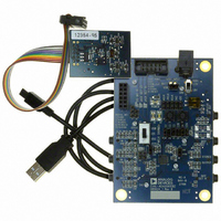
Eval Board For ADAU1761
Manufacturer
Analog Devices Inc
Series
SigmaDSP®r
Specifications of EVAL-ADAU1761Z
Main Purpose
Audio, CODEC
Embedded
Yes, DSP
Utilized Ic / Part
ADAU1761
Primary Attributes
Stereo, 24-Bit, 8 ~ 96 kHz Sampling Rate, GUI Tool
Secondary Attributes
I²C and GPIO Interfaces, 2 Differential and 1 Stereo Single-Ended Analog Inputs and Outputs
Silicon Manufacturer
Analog Devices
Core Architecture
SigmaDSP
Silicon Core Number
ADAU1761
Silicon Family Name
SigmaDSP
Application Sub Type
Audio
Lead Free Status / RoHS Status
Lead free / RoHS Compliant
Available stocks
Company
Part Number
Manufacturer
Quantity
Price
Company:

Part Number:
EVAL-ADAU1761Z
Manufacturer:
Analog Devices Inc
Quantity:
135


Jack Detection
When the JACKDET/MICIN pin is set to the jack detect func-
tion, a flag on this pin can be used to mute the line outputs
when headphones are plugged into the jack. This pin can be
configured in Register R2 (digital microphone/jack detection
control register, Address 0x4008). The JDFUNC[1:0] bits set the
functionality of the JACKDET/MICIN pin.
Additional settings for jack detection include debounce time
(JDDB[1:0] bits) and detection polarity (JDPOL bit). Because
the jack detection and digital microphone share a pin, both
functions cannot be used simultaneously.
POP-AND-CLICK SUPPRESSION
Upon power-up, precharge circuitry is enabled to suppress pops
and clicks. After power-up, the precharge circuitry can be put
into a low power mode using the POPMODE bit in Register R34
(playback pop/click suppression register, Address 0x4028).
The precharge time depends on the capacitor value on the CM
pin and the RC time constant of the load. For a typical line output
load, the precharge time is between 2 ms and 3 ms. After this
precharge time, the POPMODE bit can be set to low power mode.
Changing any register settings that affect the signal path can
cause pops and clicks on the analog outputs. To avoid these pops
and clicks, mute the appropriate outputs using Register R29 to
Register R32 (Address 0x4023 to Address 0x4026). Unmute the
analog outputs after the changes are made.
Rev. C | Page 37 of 92
LINE OUTPUTS
The line output pins (LOUTP, LOUTN, ROUTP, and ROUTN)
can be used to drive both differential and single-ended loads. In
their default settings, these pins can drive typical line loads of
10 kΩ or greater, but they can also be put into headphone mode
by setting the LOMODE bit in Register R31 (playback line output
left volume control register, Address 0x4025) and the ROMODE
bit in Register R32 (playback line output right volume control
register, Address 0x4026). In headphone mode, the line output
pins are capable of driving headphone and earpiece speakers of
16 Ω or greater. The output impedance of the line outputs is
approximately 1 kΩ.
When the line output pins are used in single-ended mode,
LOUTP and ROUTP should be used to output the signals, and
LOUTN and ROUTN should be left unconnected.
The volume controls for these outputs range from −57 dB to
+6 dB. Slew can be applied to all the playback volume controls
using the ASLEW[1:0] bits in Register R34 (playback pop/click
suppression register, Address 0x4028).
The MX5G4[1:0], MX5G3[1:0], MX6G3[1:0], and MX6G4[1:0]
bits can all provide a 6 dB gain boost to the line outputs. This
gain boost allows single-ended output signals to achieve 0 dBV
(1.0 V rms) and differential output signals to achieve up to
6 dBV (2.0 V rms). For more information, see Register R26
(playback L/R mixer left (Mixer 5) line output control register,
Address 0x4020) and Register R27 (playback L/R mixer right
(Mixer 6) line output control register, Address 0x4021).
RIGHT DAC
LEFT DAC
MIXER 3
MIXER 4
Figure 48. Differential Line Output Configuration
MX5G3[1:0]
MX6G4[1:0]
MIXER 5
MIXER 6
LOUTVOL[5:0]
ROUTVOL[5:0]
–1
–1
ADAU1761
LOUTP
LOUTN
ROUTN
ROUTP
Related parts for EVAL-ADAU1761Z
Image
Part Number
Description
Manufacturer
Datasheet
Request
R


Part Number:
Description:
BOARD EVAL FOR SI270X-A
Manufacturer:
Silicon Laboratories Inc
Datasheet:

Part Number:
Description:
BUCK CONV REF DESIGN KIT IP1201
Manufacturer:
International Rectifier
Datasheet:
Part Number:
Description:
BOARD DEMO SYNC DUAL BUCK CNVTER
Manufacturer:
International Rectifier
Datasheet:
Part Number:
Description:
BOARD DEMO SYNC BUCK CONVETER
Manufacturer:
International Rectifier
Datasheet:

Part Number:
Description:
EVALBOARD/EB Omnidirectional microphone - Analog
Manufacturer:
Analog Devices
Datasheet:
Part Number:
Description:
EVALBOARD/EB Omnidirectional microphone - Analog
Manufacturer:
Analog Devices
Datasheet:


Part Number:
Description:
BOARD EVAL LED DRIVER LT3756
Manufacturer:
Linear Technology
Datasheet:

Part Number:
Description:
BOARD EVAL FOR AD7741/7742
Manufacturer:
Analog Devices Inc
Datasheet:

Part Number:
Description:
±1.7g Dual-Axis IMEMS Accelerometer Evaluation Board
Manufacturer:
Analog Devices Inc
Datasheet:

Part Number:
Description:
IC MULTIPLIER ANALOG 8-SOIC T/R
Manufacturer:
Analog Devices Inc
Datasheet:

Part Number:
Description:
IC ANALOG MULTIPLIER 8-DIP
Manufacturer:
Analog Devices Inc
Datasheet:
Part Number:
Description:
IC ANALOG MULTIPLIER 8-SOIC
Manufacturer:
Analog Devices Inc
Datasheet:
Part Number:
Description:
IC ANALOG MULTIPLIER 8-DIP
Manufacturer:
Analog Devices Inc
Datasheet: