EVAL-ADAU1761Z Analog Devices Inc, EVAL-ADAU1761Z Datasheet - Page 52
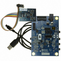
EVAL-ADAU1761Z
Manufacturer Part Number
EVAL-ADAU1761Z
Description
Eval Board For ADAU1761
Manufacturer
Analog Devices Inc
Series
SigmaDSP®r
Specifications of EVAL-ADAU1761Z
Main Purpose
Audio, CODEC
Embedded
Yes, DSP
Utilized Ic / Part
ADAU1761
Primary Attributes
Stereo, 24-Bit, 8 ~ 96 kHz Sampling Rate, GUI Tool
Secondary Attributes
I²C and GPIO Interfaces, 2 Differential and 1 Stereo Single-Ended Analog Inputs and Outputs
Silicon Manufacturer
Analog Devices
Core Architecture
SigmaDSP
Silicon Core Number
ADAU1761
Silicon Family Name
SigmaDSP
Application Sub Type
Audio
Lead Free Status / RoHS Status
Lead free / RoHS Compliant
Available stocks
Company
Part Number
Manufacturer
Quantity
Price
Company:

Part Number:
EVAL-ADAU1761Z
Manufacturer:
Analog Devices Inc
Quantity:
135


ADAU1761
Reg
R47
R48
R49
R50
R51
R52
R53
R54
R55
R56
R57
R58
R59
R60
R61
R62
R63
R64
R65
R66
CONTROL REGISTER DETAILS
All registers except for the PLL control register are 1-byte write and read registers.
R0: Clock Control, 16,384 (0x4000)
Bit 7
Table 34. Clock Control Register
Bits
3
[2:1]
0
Address
0x40C4
0x40C6
0x40C7
0x40C8
0x40C9
0x40D0
0x40D1
0x40D2
0x40D3
0x40D4
0x40EB
0x40F2
0x40F3
0x40F4
0x40F5
0x40F6
0x40F7
0x40F8
0x40F9
0x40FA
Bit Name
CLKSRC
INFREQ[1:0]
COREN
Bit 6
Name
CRC enable
GPIO0 pin control
GPIO1 pin control
GPIO2 pin control
GPIO3 pin control
Watchdog enable
Watchdog value
Watchdog error
DSP sampling rate
setting
Serial input route
control
Serial output route
control
Serial data/GPIO
pin configuration
DSP enable
DSP run
DSP slew modes
Serial port
sampling rate
Clock Enable 0
Clock Enable 1
Description
Clock source select.
0 = direct from MCLK pin (default).
1 = PLL clock.
Input clock frequency. Sets the core clock rate that generates the core clock. If the PLL is used, this value is
automatically set to 1024 × f
Setting
00
01
10
11
Core clock enable. Only the R0 and R1 registers can be accessed when this bit is set to 0 (core clock disabled).
0 = core clock disabled (default).
1 = core clock enabled.
Reserved
Bit 5
Bit 7
Reserved
Reserved
Bit 6
SLEWPD
Bit 4
Reserved
Reserved
Reserved
Reserved
Reserved
Reserved
Reserved
Reserved
S
.
Input Clock Frequency
256 × f
512 × f
768 × f
1024 × f
Bit 5
ALCPD
Rev. C | Page 52 of 92
Reserved
Reserved
S
S
S
(default)
S
Bit 3
CLKSRC
Bit 4
MOSLW
DECPD
Reserved
Reserved
Reserved
Reserved
Reserved
DOG[23:16]
DOG[15:8]
DOG[7:0]
Bit 3
LRGP3
ROSLW
SOUTPD
Bit 2
Bit 2
BGP2
LOSLW
INTPD
INFREQ[1:0]
SOUTRT[3:0]
DSPSR[3:0]
GPIO0[3:0]
GPIO1[3:0]
GPIO2[3:0]
GPIO3[3:0]
SINRT[3:0]
Bit 1
Bit 1
SDOGP1
RHPSLW
SINPD
CLK1
SPSR[2:0]
Bit 0
CRCEN
DOGEN
DOGER
SDIGP0
DSPEN
DSPRUN
LHPSLW
SPPD
CLK0
Bit 0
COREN
Default
00000000
00000000
00000000
00000000
00000000
00000000
00000000
00000000
00000000
00000000
00000001
00000000
00000000
00000000
00000000
00000000
00000000
00000000
00000000
00000000
Related parts for EVAL-ADAU1761Z
Image
Part Number
Description
Manufacturer
Datasheet
Request
R


Part Number:
Description:
BOARD EVAL FOR SI270X-A
Manufacturer:
Silicon Laboratories Inc
Datasheet:

Part Number:
Description:
BUCK CONV REF DESIGN KIT IP1201
Manufacturer:
International Rectifier
Datasheet:
Part Number:
Description:
BOARD DEMO SYNC DUAL BUCK CNVTER
Manufacturer:
International Rectifier
Datasheet:
Part Number:
Description:
BOARD DEMO SYNC BUCK CONVETER
Manufacturer:
International Rectifier
Datasheet:

Part Number:
Description:
EVALBOARD/EB Omnidirectional microphone - Analog
Manufacturer:
Analog Devices
Datasheet:
Part Number:
Description:
EVALBOARD/EB Omnidirectional microphone - Analog
Manufacturer:
Analog Devices
Datasheet:


Part Number:
Description:
BOARD EVAL LED DRIVER LT3756
Manufacturer:
Linear Technology
Datasheet:

Part Number:
Description:
BOARD EVAL FOR AD7741/7742
Manufacturer:
Analog Devices Inc
Datasheet:

Part Number:
Description:
±1.7g Dual-Axis IMEMS Accelerometer Evaluation Board
Manufacturer:
Analog Devices Inc
Datasheet:

Part Number:
Description:
IC MULTIPLIER ANALOG 8-SOIC T/R
Manufacturer:
Analog Devices Inc
Datasheet:

Part Number:
Description:
IC ANALOG MULTIPLIER 8-DIP
Manufacturer:
Analog Devices Inc
Datasheet:
Part Number:
Description:
IC ANALOG MULTIPLIER 8-SOIC
Manufacturer:
Analog Devices Inc
Datasheet:
Part Number:
Description:
IC ANALOG MULTIPLIER 8-DIP
Manufacturer:
Analog Devices Inc
Datasheet: