EP1S80B956C7N Altera, EP1S80B956C7N Datasheet - Page 3
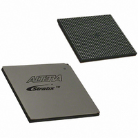
EP1S80B956C7N
Manufacturer Part Number
EP1S80B956C7N
Description
IC STRATIX FPGA 80K LE 956-BGA
Manufacturer
Altera
Series
Stratix®r
Datasheet
1.EP1S10F484I6N.pdf
(864 pages)
Specifications of EP1S80B956C7N
Number Of Logic Elements/cells
79040
Number Of Labs/clbs
7904
Total Ram Bits
7427520
Number Of I /o
683
Voltage - Supply
1.425 V ~ 1.575 V
Mounting Type
Surface Mount
Operating Temperature
0°C ~ 85°C
Package / Case
956-BGA
Lead Free Status / RoHS Status
Lead free / RoHS Compliant
Number Of Gates
-
Available stocks
Company
Part Number
Manufacturer
Quantity
Price


Chapter Revision Dates .......................................................................... vii
About This Handbook .............................................................................. ix
Section I. Stratix Device Family Data Sheet
Chapter 1. Introduction
Chapter 2. Stratix Architecture
Altera Corporation
How to Find Information ........................................................................................................................ ix
How to Contact Altera ............................................................................................................................. ix
Typographic Conventions ........................................................................................................................ x
Revision History ............................................................................................................................ Part I–1
Introduction ............................................................................................................................................ 1–1
Features ................................................................................................................................................... 1–2
Functional Description .......................................................................................................................... 2–1
Logic Array Blocks ................................................................................................................................ 2–3
Logic Elements ....................................................................................................................................... 2–6
MultiTrack Interconnect ..................................................................................................................... 2–14
TriMatrix Memory ............................................................................................................................... 2–21
LAB Interconnects ............................................................................................................................ 2–4
LAB Control Signals ......................................................................................................................... 2–5
LUT Chain & Register Chain .......................................................................................................... 2–8
addnsub Signal ................................................................................................................................. 2–8
LE Operating Modes ........................................................................................................................ 2–8
Clear & Preset Logic Control ........................................................................................................ 2–13
Memory Modes ............................................................................................................................... 2–22
Clear Signals .................................................................................................................................... 2–24
Parity Bit Support ........................................................................................................................... 2–24
Shift Register Support .................................................................................................................... 2–25
Memory Block Size ......................................................................................................................... 2–26
Independent Clock Mode .............................................................................................................. 2–44
Input/Output Clock Mode ........................................................................................................... 2–46
Read/Write Clock Mode ............................................................................................................... 2–49
Single-Port Mode ............................................................................................................................ 2–51
Multiplier Block .............................................................................................................................. 2–57
Adder/Output Blocks ................................................................................................................... 2–61
Modes of Operation ....................................................................................................................... 2–64
Contents
iii
Related parts for EP1S80B956C7N
Image
Part Number
Description
Manufacturer
Datasheet
Request
R

Part Number:
Description:
CYCLONE II STARTER KIT EP2C20N
Manufacturer:
Altera
Datasheet:


Part Number:
Description:
CPLD, EP610 Family, ECMOS Process, 300 Gates, 16 Macro Cells, 16 Reg., 16 User I/Os, 5V Supply, 35 Speed Grade, 24DIP
Manufacturer:
Altera Corporation
Datasheet:
Part Number:
Description:
CPLD, EP610 Family, ECMOS Process, 300 Gates, 16 Macro Cells, 16 Reg., 16 User I/Os, 5V Supply, 15 Speed Grade, 24DIP
Manufacturer:
Altera Corporation
Datasheet:
Part Number:
Description:
Manufacturer:
Altera Corporation
Datasheet:
Part Number:
Description:
CPLD, EP610 Family, ECMOS Process, 300 Gates, 16 Macro Cells, 16 Reg., 16 User I/Os, 5V Supply, 30 Speed Grade, 24DIP
Manufacturer:
Altera Corporation
Datasheet:
Part Number:
Description:
High-performance, low-power erasable programmable logic devices with 8 macrocells, 10ns
Manufacturer:
Altera Corporation
Datasheet:
Part Number:
Description:
High-performance, low-power erasable programmable logic devices with 8 macrocells, 7ns
Manufacturer:
Altera Corporation
Datasheet:
Part Number:
Description:
Classic EPLD
Manufacturer:
Altera Corporation
Datasheet:
Part Number:
Description:
High-performance, low-power erasable programmable logic devices with 8 macrocells, 10ns
Manufacturer:
Altera Corporation
Datasheet:
Part Number:
Description:
Manufacturer:
Altera Corporation
Datasheet:
Part Number:
Description:
Manufacturer:
Altera Corporation
Datasheet:
Part Number:
Description:
Manufacturer:
Altera Corporation
Datasheet:
Part Number:
Description:
CPLD, EP610 Family, ECMOS Process, 300 Gates, 16 Macro Cells, 16 Reg., 16 User I/Os, 5V Supply, 25 Speed Grade, 24DIP
Manufacturer:
Altera Corporation
Datasheet: