EP1S80B956C7N Altera, EP1S80B956C7N Datasheet - Page 536
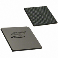
EP1S80B956C7N
Manufacturer Part Number
EP1S80B956C7N
Description
IC STRATIX FPGA 80K LE 956-BGA
Manufacturer
Altera
Series
Stratix®r
Datasheet
1.EP1S10F484I6N.pdf
(864 pages)
Specifications of EP1S80B956C7N
Number Of Logic Elements/cells
79040
Number Of Labs/clbs
7904
Total Ram Bits
7427520
Number Of I /o
683
Voltage - Supply
1.425 V ~ 1.575 V
Mounting Type
Surface Mount
Operating Temperature
0°C ~ 85°C
Package / Case
956-BGA
Lead Free Status / RoHS Status
Lead free / RoHS Compliant
Number Of Gates
-
Available stocks
Company
Part Number
Manufacturer
Quantity
Price


Software Support
5–64
Stratix Device Handbook, Volume 2
Data Realignment
Check the Use the “rx_data_align” input port box within the Input Ports
box to add the rx_data_align output port and enable the data
realignment circuitry in Stratix SERDES. See
Realignment” on page 5–25
create a state machine to send a pulse to the rx_data_align port to
realign the data coming in the LVDS receiver. You need to assert the port
for at least two clock cycles to enable the data realignment circuitry. Go
to the Altera web site at www.altera.com for a sample design written in
Verilog HDL.
For guaranteed performance when using data realignment, check the
Add Extra registers for rx_data_align input box when using the
rx_data_align port. The Quartus II software places one
synchronization register in the LE closest to the rx_data_align port.
Register Outputs
Check the Register outputs box to register the receiver’s output data. The
register acts as the module’s register boundary. If the module fed by the
receiver does not have a register boundary for the data, turn this option
on. The number of registers used is proportional to the deserialization
factor (J). The Quartus II software places the synchronization registers in
the LEs closest to the SERDES circuitry.
Use Common PLL for Both Transmitter & Receiver
Check the Use Common PLLs for Rx and Tx box to place both the LVDS
transmitter and the LVDS receiver in the same Stratix device I/O bank.
The Quartus II software allows the transmitter and receiver to share the
same fast PLL when they use the same input clock. Although you must
separate the transmitter and receiver modules in your design, the
Quartus II software merges the fast PLLs when appropriate and give you
the following message:
Receiver fast PLL <lvds_rx PLL name> and transmitter fast PLL <lvds_tx
PLL name> are merged together
The Quartus II software provides the following message when it cannot
merge the fast PLLs for the LVDS transmitter and receiver pair in the
design:
Can't merge transmitter-only fast PLL <lvds_tx PLL name> and receiver-
only fast PLL <lvds_rx PLL name>
rx_outclock Resource
You can use either the global or regional clock for the rx_outclock
signal. If you select Auto in the Quartus II software, the tool uses any
available lines.
for more information. If necessary, you can
“Receiver Data
Altera Corporation
July 2005
Related parts for EP1S80B956C7N
Image
Part Number
Description
Manufacturer
Datasheet
Request
R

Part Number:
Description:
CYCLONE II STARTER KIT EP2C20N
Manufacturer:
Altera
Datasheet:


Part Number:
Description:
CPLD, EP610 Family, ECMOS Process, 300 Gates, 16 Macro Cells, 16 Reg., 16 User I/Os, 5V Supply, 35 Speed Grade, 24DIP
Manufacturer:
Altera Corporation
Datasheet:
Part Number:
Description:
CPLD, EP610 Family, ECMOS Process, 300 Gates, 16 Macro Cells, 16 Reg., 16 User I/Os, 5V Supply, 15 Speed Grade, 24DIP
Manufacturer:
Altera Corporation
Datasheet:
Part Number:
Description:
Manufacturer:
Altera Corporation
Datasheet:
Part Number:
Description:
CPLD, EP610 Family, ECMOS Process, 300 Gates, 16 Macro Cells, 16 Reg., 16 User I/Os, 5V Supply, 30 Speed Grade, 24DIP
Manufacturer:
Altera Corporation
Datasheet:
Part Number:
Description:
High-performance, low-power erasable programmable logic devices with 8 macrocells, 10ns
Manufacturer:
Altera Corporation
Datasheet:
Part Number:
Description:
High-performance, low-power erasable programmable logic devices with 8 macrocells, 7ns
Manufacturer:
Altera Corporation
Datasheet:
Part Number:
Description:
Classic EPLD
Manufacturer:
Altera Corporation
Datasheet:
Part Number:
Description:
High-performance, low-power erasable programmable logic devices with 8 macrocells, 10ns
Manufacturer:
Altera Corporation
Datasheet:
Part Number:
Description:
Manufacturer:
Altera Corporation
Datasheet:
Part Number:
Description:
Manufacturer:
Altera Corporation
Datasheet:
Part Number:
Description:
Manufacturer:
Altera Corporation
Datasheet:
Part Number:
Description:
CPLD, EP610 Family, ECMOS Process, 300 Gates, 16 Macro Cells, 16 Reg., 16 User I/Os, 5V Supply, 25 Speed Grade, 24DIP
Manufacturer:
Altera Corporation
Datasheet: