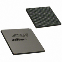
EP1S80B956C7N Altera, EP1S80B956C7N Datasheet - Page 347

EP1S80B956C7N
Manufacturer Part Number
EP1S80B956C7N
Description
IC STRATIX FPGA 80K LE 956-BGA
Manufacturer
Altera
Series
Stratix®r
Datasheet
1.EP1S10F484I6N.pdf
(864 pages)
Specifications of EP1S80B956C7N
Number Of Logic Elements/cells
79040
Number Of Labs/clbs
7904
Total Ram Bits
7427520
Number Of I /o
683
Voltage - Supply
1.425 V ~ 1.575 V
Mounting Type
Surface Mount
Operating Temperature
0°C ~ 85°C
Package / Case
956-BGA
Lead Free Status / RoHS Status
Lead free / RoHS Compliant
Number Of Gates
-
Available stocks
Company
Part Number
Manufacturer
Quantity
Price
- Current page: 347 of 864
- Download datasheet (11Mb)
Altera Corporation
July 2005
CLK0p/n
CLK1p/n
CLK2p/n
CLK3p/n
CLK8p/n
CLK9p/n
CLK10p/n
CLK11p/n
FPLL7CLKp/n
FPLL8CLKp/n
FPLL9CLKp/n
FPLL10CLKp/n
PLLENABLE
VCCA_PLL1
Table 1–13. Fast PLL Pins (Part 1 of 3)
Pin
resynchronizes to its input clock as it relocks. If the target VCO frequency
is below this nominal frequency, then the output frequency starts at a
higher value then desired as it locks.
The pfdena signals control the PFD output with a programmable gate. If
you disable the PFD, the VCO operates at its last set value of control
voltage and frequency with some long-term drift to a lower frequency.
The system continues running when the PLL goes out of lock or the input
clock disables. By maintaining the last locked frequency, the system has
time to store its current settings before shutting down.
If the PLL loses lock for any reason (for example, because of excessive
inclk jitter, clock switchover, PLL reconfiguration, or power supply
noise), the PLL must be reset with the areset signal to guarantee correct
phase relationship between the PLL output clocks. If the phase
relationship between the input clock and the output clock and between
different output clocks from the PLL is not important in your design, it is
not necessary to reset the PLL.
Pins
Table 1–13
For inclk port connections to pins see
Single-ended or differential pins that can drive the inclk port for PLL 1 or 7.
Single-ended or differential pins that can drive the inclk port for PLL 1.
Single-ended or differential pins that can drive the inclk port for PLL 2 or 8.
Single-ended or differential pins that can drive the inclk port for PLL 2.
Single-ended or differential pins that can drive the inclk port for PLL 3 or 9.
Single-ended or differential pins that can drive the inclk port for PLL 3.
Single-ended or differential pins that can drive the inclk port for PLL 4 or 10.
Single-ended or differential pins that can drive the inclk port for PLL 4.
Single-ended or differential pins that can drive the inclk port for PLL 7.
Single-ended or differential pins that can drive the inclk port for PLL 8.
Single-ended or differential pins that can drive the inclk port for PLL 9.
Single-ended or differential pins that can drive the inclk port for PLL 10.
Dedicated input pin that drives the pllena port of all or a set of PLLs. If you do not
use this pin, connect it to ground.
Analog power for PLL 1. Connect this pin to 1.5 V, even if the PLL is not used.
shows the physical pins and their purpose for the Fast PLLs.
General-Purpose PLLs in Stratix & Stratix GX Devices
Description
“Clocking” on page
Stratix Device Handbook, Volume 2
1–39.
(1)
(1)
(1)
(1)
(1)
1–37
(1)
Related parts for EP1S80B956C7N
Image
Part Number
Description
Manufacturer
Datasheet
Request
R

Part Number:
Description:
CYCLONE II STARTER KIT EP2C20N
Manufacturer:
Altera
Datasheet:

Part Number:
Description:
CPLD, EP610 Family, ECMOS Process, 300 Gates, 16 Macro Cells, 16 Reg., 16 User I/Os, 5V Supply, 35 Speed Grade, 24DIP
Manufacturer:
Altera Corporation
Datasheet:

Part Number:
Description:
CPLD, EP610 Family, ECMOS Process, 300 Gates, 16 Macro Cells, 16 Reg., 16 User I/Os, 5V Supply, 15 Speed Grade, 24DIP
Manufacturer:
Altera Corporation
Datasheet:

Part Number:
Description:
Manufacturer:
Altera Corporation
Datasheet:

Part Number:
Description:
CPLD, EP610 Family, ECMOS Process, 300 Gates, 16 Macro Cells, 16 Reg., 16 User I/Os, 5V Supply, 30 Speed Grade, 24DIP
Manufacturer:
Altera Corporation
Datasheet:

Part Number:
Description:
High-performance, low-power erasable programmable logic devices with 8 macrocells, 10ns
Manufacturer:
Altera Corporation
Datasheet:

Part Number:
Description:
High-performance, low-power erasable programmable logic devices with 8 macrocells, 7ns
Manufacturer:
Altera Corporation
Datasheet:

Part Number:
Description:
Classic EPLD
Manufacturer:
Altera Corporation
Datasheet:

Part Number:
Description:
High-performance, low-power erasable programmable logic devices with 8 macrocells, 10ns
Manufacturer:
Altera Corporation
Datasheet:

Part Number:
Description:
Manufacturer:
Altera Corporation
Datasheet:

Part Number:
Description:
Manufacturer:
Altera Corporation
Datasheet:

Part Number:
Description:
Manufacturer:
Altera Corporation
Datasheet:

Part Number:
Description:
CPLD, EP610 Family, ECMOS Process, 300 Gates, 16 Macro Cells, 16 Reg., 16 User I/Os, 5V Supply, 25 Speed Grade, 24DIP
Manufacturer:
Altera Corporation
Datasheet:


