EP1S80B956C7N Altera, EP1S80B956C7N Datasheet - Page 773
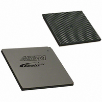
EP1S80B956C7N
Manufacturer Part Number
EP1S80B956C7N
Description
IC STRATIX FPGA 80K LE 956-BGA
Manufacturer
Altera
Series
Stratix®r
Datasheet
1.EP1S10F484I6N.pdf
(864 pages)
Specifications of EP1S80B956C7N
Number Of Logic Elements/cells
79040
Number Of Labs/clbs
7904
Total Ram Bits
7427520
Number Of I /o
683
Voltage - Supply
1.425 V ~ 1.575 V
Mounting Type
Surface Mount
Operating Temperature
0°C ~ 85°C
Package / Case
956-BGA
Lead Free Status / RoHS Status
Lead free / RoHS Compliant
Number Of Gates
-
Available stocks
Company
Part Number
Manufacturer
Quantity
Price


Altera Corporation
July 2005
nCEO
DCLK
DATA0
Table 11–15. Dedicated Configuration Pins on the Stratix or Stratix GX Device
Pin Name
N/A
N/A
I/O
User Mode
All Multi-
Device
Schemes
Synchronous
configuration
schemes
(PS, FPP)
PS, FPP, PPA Input
Configuration
Scheme
Output
Input
(PS, FPP)
Pin Type
Output that drives low when device
configuration is complete. In single device
configuration, this pin is left floating. In multi-
device configuration, this pin feeds the next
device’s
in the chain is left floating.
The voltage levels driven out by this pin are
dependent on the V
resides in.
In PS and FPP configuration,
input used to clock data from an external
source into the target device. Data is latched
into the FPGA on the rising edge of
In PPA mode,
to prevent this pin from floating.
After configuration, this pin is tri-stated. In
schemes that use a configuration device,
DCLK
In schemes that use a control host,
should be driven either high or low, whichever
is more convenient. Toggling this pin after
configuration does not affect the configured
device. This pin uses Schmitt trigger input
buffers.
Data input. In serial configuration modes, bit-
wide configuration data is presented to the
target device on the
V
V
After configuration,
user I/O and the state of this pin depends on
the Dual-Purpose Pin settings.
After configuration, EPC1 and EPC1441
devices tri-state this pin, while enhanced
configuration and EPC2 devices drive this pin
high.
I L
C C I O
Configuring Stratix & Stratix GX Devices
levels for this pin are dependent on the
is driven low after configuration is done.
of the I/O bank that it resides in.
nCE
Stratix Device Handbook, Volume 2
pin. The
DCLK
Description
DATA0
C C I O
should be tied high to V
DATA0
(Part 5 of 8)
nCEO
of the I/O bank it
is available as a
pin. The V
of the last device
DCLK
is the clock
DCLK
DCLK
I H
11–55
and
.
C C
Related parts for EP1S80B956C7N
Image
Part Number
Description
Manufacturer
Datasheet
Request
R

Part Number:
Description:
CYCLONE II STARTER KIT EP2C20N
Manufacturer:
Altera
Datasheet:


Part Number:
Description:
CPLD, EP610 Family, ECMOS Process, 300 Gates, 16 Macro Cells, 16 Reg., 16 User I/Os, 5V Supply, 35 Speed Grade, 24DIP
Manufacturer:
Altera Corporation
Datasheet:
Part Number:
Description:
CPLD, EP610 Family, ECMOS Process, 300 Gates, 16 Macro Cells, 16 Reg., 16 User I/Os, 5V Supply, 15 Speed Grade, 24DIP
Manufacturer:
Altera Corporation
Datasheet:
Part Number:
Description:
Manufacturer:
Altera Corporation
Datasheet:
Part Number:
Description:
CPLD, EP610 Family, ECMOS Process, 300 Gates, 16 Macro Cells, 16 Reg., 16 User I/Os, 5V Supply, 30 Speed Grade, 24DIP
Manufacturer:
Altera Corporation
Datasheet:
Part Number:
Description:
High-performance, low-power erasable programmable logic devices with 8 macrocells, 10ns
Manufacturer:
Altera Corporation
Datasheet:
Part Number:
Description:
High-performance, low-power erasable programmable logic devices with 8 macrocells, 7ns
Manufacturer:
Altera Corporation
Datasheet:
Part Number:
Description:
Classic EPLD
Manufacturer:
Altera Corporation
Datasheet:
Part Number:
Description:
High-performance, low-power erasable programmable logic devices with 8 macrocells, 10ns
Manufacturer:
Altera Corporation
Datasheet:
Part Number:
Description:
Manufacturer:
Altera Corporation
Datasheet:
Part Number:
Description:
Manufacturer:
Altera Corporation
Datasheet:
Part Number:
Description:
Manufacturer:
Altera Corporation
Datasheet:
Part Number:
Description:
CPLD, EP610 Family, ECMOS Process, 300 Gates, 16 Macro Cells, 16 Reg., 16 User I/Os, 5V Supply, 25 Speed Grade, 24DIP
Manufacturer:
Altera Corporation
Datasheet: