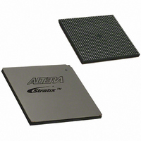
EP1S80B956C7N Altera, EP1S80B956C7N Datasheet - Page 366

EP1S80B956C7N
Manufacturer Part Number
EP1S80B956C7N
Description
IC STRATIX FPGA 80K LE 956-BGA
Manufacturer
Altera
Series
Stratix®r
Datasheet
1.EP1S10F484I6N.pdf
(864 pages)
Specifications of EP1S80B956C7N
Number Of Logic Elements/cells
79040
Number Of Labs/clbs
7904
Total Ram Bits
7427520
Number Of I /o
683
Voltage - Supply
1.425 V ~ 1.575 V
Mounting Type
Surface Mount
Operating Temperature
0°C ~ 85°C
Package / Case
956-BGA
Lead Free Status / RoHS Status
Lead free / RoHS Compliant
Number Of Gates
-
Available stocks
Company
Part Number
Manufacturer
Quantity
Price
- Current page: 366 of 864
- Download datasheet (11Mb)
Conclusion
Conclusion
1–56
Stratix Device Handbook, Volume 2
Guidelines
Use the following guidelines for optimal jitter performance on the
external clock outputs from enhanced PLLs 5 and 6. If all outputs are
running at the same frequency, these guidelines are not necessary to
improve performance.
■
■
■
■
Stratix and Stratix GX device enhanced PLLs provide you with complete
control of your clocks and system timing. These PLLs are capable of
offering flexible system level clock management that was previously only
available in discrete PLL devices. The embedded PLLs meet and exceed
the features offered by these high-end discrete devices, reducing the need
for other timing devices in the system.
When driving two or more clock outputs from PLL 5 or 6, separate
the outputs into the two groups shown in
if you are driving 100- and 200-MHz clock outputs off-chip from PLL
5, place one output on PLL5_OUT0p (powered by VCC_PLL5_OUTA)
and the other output on PLL5_OUT2p (powered by
VCC_PLL5_OUTB). Since the output buffers are powered by different
pins, they are less susceptible to bimodal jitter. Bimodal jitter is a
deterministic jitter not caused by the PLL but rather by coincident
edges of clock outputs that are multiples of each other.
Use phase shift to ensure edges are not coincident on all the clock
outputs.
Use phase shift to skew clock edges with respect to each other for
best jitter performance.
1
If you cannot drive multiple clocks of different frequencies and
phase shifts or isolate banks, you should control the drive capability
on the lower frequency clock. Reducing how much current the
output buffer has to supply can reduce the noise. Minimize
capacitive load on the slower frequency output and configure the
output buffer to drive slow slew rate and lower current strength. The
higher frequency output should have an improved performance, but
this may degrade the performance of your lower frequency clock
output.
Delay shift (time delay elements) are no longer supported
in Stratix PLLs. Use the phase shift feature to implement the
desired time shift.
Figure
1–24. For example,
Altera Corporation
July 2005
Related parts for EP1S80B956C7N
Image
Part Number
Description
Manufacturer
Datasheet
Request
R

Part Number:
Description:
CYCLONE II STARTER KIT EP2C20N
Manufacturer:
Altera
Datasheet:

Part Number:
Description:
CPLD, EP610 Family, ECMOS Process, 300 Gates, 16 Macro Cells, 16 Reg., 16 User I/Os, 5V Supply, 35 Speed Grade, 24DIP
Manufacturer:
Altera Corporation
Datasheet:

Part Number:
Description:
CPLD, EP610 Family, ECMOS Process, 300 Gates, 16 Macro Cells, 16 Reg., 16 User I/Os, 5V Supply, 15 Speed Grade, 24DIP
Manufacturer:
Altera Corporation
Datasheet:

Part Number:
Description:
Manufacturer:
Altera Corporation
Datasheet:

Part Number:
Description:
CPLD, EP610 Family, ECMOS Process, 300 Gates, 16 Macro Cells, 16 Reg., 16 User I/Os, 5V Supply, 30 Speed Grade, 24DIP
Manufacturer:
Altera Corporation
Datasheet:

Part Number:
Description:
High-performance, low-power erasable programmable logic devices with 8 macrocells, 10ns
Manufacturer:
Altera Corporation
Datasheet:

Part Number:
Description:
High-performance, low-power erasable programmable logic devices with 8 macrocells, 7ns
Manufacturer:
Altera Corporation
Datasheet:

Part Number:
Description:
Classic EPLD
Manufacturer:
Altera Corporation
Datasheet:

Part Number:
Description:
High-performance, low-power erasable programmable logic devices with 8 macrocells, 10ns
Manufacturer:
Altera Corporation
Datasheet:

Part Number:
Description:
Manufacturer:
Altera Corporation
Datasheet:

Part Number:
Description:
Manufacturer:
Altera Corporation
Datasheet:

Part Number:
Description:
Manufacturer:
Altera Corporation
Datasheet:

Part Number:
Description:
CPLD, EP610 Family, ECMOS Process, 300 Gates, 16 Macro Cells, 16 Reg., 16 User I/Os, 5V Supply, 25 Speed Grade, 24DIP
Manufacturer:
Altera Corporation
Datasheet:


