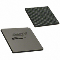
EP1S80B956C7N Altera, EP1S80B956C7N Datasheet - Page 514

EP1S80B956C7N
Manufacturer Part Number
EP1S80B956C7N
Description
IC STRATIX FPGA 80K LE 956-BGA
Manufacturer
Altera
Series
Stratix®r
Datasheet
1.EP1S10F484I6N.pdf
(864 pages)
Specifications of EP1S80B956C7N
Number Of Logic Elements/cells
79040
Number Of Labs/clbs
7904
Total Ram Bits
7427520
Number Of I /o
683
Voltage - Supply
1.425 V ~ 1.575 V
Mounting Type
Surface Mount
Operating Temperature
0°C ~ 85°C
Package / Case
956-BGA
Lead Free Status / RoHS Status
Lead free / RoHS Compliant
Number Of Gates
-
Available stocks
Company
Part Number
Manufacturer
Quantity
Price
- Current page: 514 of 864
- Download datasheet (11Mb)
SERDES Bypass DDR Differential Signaling
SERDES Bypass
DDR Differential
Signaling
5–42
Stratix Device Handbook, Volume 2
Switching Characteristics
Timing specifications for Stratix devices are listed in
You can also find Stratix device timing information in the Stratix Device
Family Data Sheet section of the Stratix Device Handbook, Volume 1.
Timing Analysis
Differential timing analysis is based on skew between data and the clock
signals. For static timing analysis, the timing characteristics of the
differential I/O standards are guaranteed by design and depend on the
frequency at which they are operated. Use the values in the Stratix Device
Family Data Sheet section of the Stratix Device Handbook, Volume 1 to
calculate system timing margins for various I/O protocols. For detailed
descriptions and implementations of these protocols, see the Altera web
site at www.altera.com.
Each Stratix device high-speed differential I/O channel can transmit or
receive data in by-two (
pins do not require dedicated SERDES circuitry and they implement
serialization and deserialization with minimal logic.
SERDES Bypass DDR Differential Interface Review
Stratix devices use dedicated DDR circuitry to implement
signaling. Although SDR circuitry samples data only at the positive edge
of the clock, DDR captures data on both the rising and falling edges for
twice the transfer rate of SDR. Stratix device shift registers, internal global
PLLs, and I/O cells can perform serial-to-parallel conversions on
incoming data and parallel-to-serial conversion on outgoing data.
SERDES Clock Domains
The SERDES bypass differential signaling can use any of the many clock
domains available in Stratix devices. These clock domains fall into four
categories: global, regional, fast regional, and internally generated.
General-purpose PLLs generate the global clock domains. The fast PLLs
can generate additional global clocks domains. Each PLL features two
taps that directly drive two unique global clock networks. A dedicated
clock pin drives each general-purpose PLL. These clock lines are utilized
when designing for speeds up to 420 Mbps.
page
5–19, respectively, show the available clocks in Stratix devices.
×
2) mode at up to 624 Mbps using PLLs. These
Tables 5–3
Tables 5–7
Altera Corporation
and
×
2 differential
5–4
on
and 5–8.
July 2005
Related parts for EP1S80B956C7N
Image
Part Number
Description
Manufacturer
Datasheet
Request
R

Part Number:
Description:
CYCLONE II STARTER KIT EP2C20N
Manufacturer:
Altera
Datasheet:

Part Number:
Description:
CPLD, EP610 Family, ECMOS Process, 300 Gates, 16 Macro Cells, 16 Reg., 16 User I/Os, 5V Supply, 35 Speed Grade, 24DIP
Manufacturer:
Altera Corporation
Datasheet:

Part Number:
Description:
CPLD, EP610 Family, ECMOS Process, 300 Gates, 16 Macro Cells, 16 Reg., 16 User I/Os, 5V Supply, 15 Speed Grade, 24DIP
Manufacturer:
Altera Corporation
Datasheet:

Part Number:
Description:
Manufacturer:
Altera Corporation
Datasheet:

Part Number:
Description:
CPLD, EP610 Family, ECMOS Process, 300 Gates, 16 Macro Cells, 16 Reg., 16 User I/Os, 5V Supply, 30 Speed Grade, 24DIP
Manufacturer:
Altera Corporation
Datasheet:

Part Number:
Description:
High-performance, low-power erasable programmable logic devices with 8 macrocells, 10ns
Manufacturer:
Altera Corporation
Datasheet:

Part Number:
Description:
High-performance, low-power erasable programmable logic devices with 8 macrocells, 7ns
Manufacturer:
Altera Corporation
Datasheet:

Part Number:
Description:
Classic EPLD
Manufacturer:
Altera Corporation
Datasheet:

Part Number:
Description:
High-performance, low-power erasable programmable logic devices with 8 macrocells, 10ns
Manufacturer:
Altera Corporation
Datasheet:

Part Number:
Description:
Manufacturer:
Altera Corporation
Datasheet:

Part Number:
Description:
Manufacturer:
Altera Corporation
Datasheet:

Part Number:
Description:
Manufacturer:
Altera Corporation
Datasheet:

Part Number:
Description:
CPLD, EP610 Family, ECMOS Process, 300 Gates, 16 Macro Cells, 16 Reg., 16 User I/Os, 5V Supply, 25 Speed Grade, 24DIP
Manufacturer:
Altera Corporation
Datasheet:


