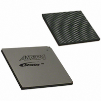
EP1S80B956C7N Altera, EP1S80B956C7N Datasheet - Page 398

EP1S80B956C7N
Manufacturer Part Number
EP1S80B956C7N
Description
IC STRATIX FPGA 80K LE 956-BGA
Manufacturer
Altera
Series
Stratix®r
Datasheet
1.EP1S10F484I6N.pdf
(864 pages)
Specifications of EP1S80B956C7N
Number Of Logic Elements/cells
79040
Number Of Labs/clbs
7904
Total Ram Bits
7427520
Number Of I /o
683
Voltage - Supply
1.425 V ~ 1.575 V
Mounting Type
Surface Mount
Operating Temperature
0°C ~ 85°C
Package / Case
956-BGA
Lead Free Status / RoHS Status
Lead free / RoHS Compliant
Number Of Gates
-
Available stocks
Company
Part Number
Manufacturer
Quantity
Price
- Current page: 398 of 864
- Download datasheet (11Mb)
External Memory Standards
3–2
Stratix Device Handbook, Volume 2
f
Interface Pins
DDR devices use interface pins including data, data strobe, clock,
command, and address pins. Data is sent and captured at twice the clock
rate by transferring data on both the positive and negative edge of a clock.
The commands and addresses only use one active edge of a clock.
Connect the memory device’s DQ and DQS pins to the DQ and DQS pins,
respectively, as listed in the Stratix and Stratix GX devices pin table. DDR
SDRAM also uses active-high data mask pins for writes. You can connect
DM pins to any of the I/O pins in the same bank as the DQ pins of the
FPGA. There is one DM pin per DQS/DQ group.
DDR SDRAM ×16 devices use two DQS pins, and each DQS pin is
associated with eight DQ pins. However, this is not the same as the
×16 mode in Stratix and Stratix GX devices. To support a ×16 DDR
SDRAM, you need to configure the Stratix and Stratix GX FPGAs to use
two sets of DQ pins in ×8 mode. Similarly if your ×32 memory device uses
four DQS pins where each DQS pin is associated with eight DQ pins, you
need to configure the Stratix and Stratix GX FPGA to use four sets of pins
in ×8 mode.
You can also use any I/O pins in banks 1, 2, 5, or 6 to interface with
DDR SDRAM devices. These banks do not have dedicated circuitry,
though.
You can also use any of the user I/O pins for commands and addresses to
the DDR SDRAM.
For more information, see AN 342: Interfacing DDR SDRAM with Stratix
& Stratix GX Devices.
If the DDR SDRAM device supports ECC, the design uses a DQS/DQ
group for ECC pins. You can use any of the user I/O pins for commands
and addresses.
Because of the symmetrical setup and hold time for the command and
address pins at the memory, you might need to generate these signals
from the system clock’s negative edge.
The clocks to the SDRAM device are called CK and CK#. Use any of the
user I/O pins via the DDR registers to generate the CK and CK# signals
to meet the DDR SDRAM t
requires that the DQS signal’s positive edge write operations must be
within 25% of the positive edge of the DDR SDRAM clock input. Using
user I/O pins for CK and CK# ensures that any PVT variations seen by
the DQS signal are tracked by these pins, too.
DQSS
requirement. The memory device’s t
Altera Corporation
June 2006
DQSS
Related parts for EP1S80B956C7N
Image
Part Number
Description
Manufacturer
Datasheet
Request
R

Part Number:
Description:
CYCLONE II STARTER KIT EP2C20N
Manufacturer:
Altera
Datasheet:

Part Number:
Description:
CPLD, EP610 Family, ECMOS Process, 300 Gates, 16 Macro Cells, 16 Reg., 16 User I/Os, 5V Supply, 35 Speed Grade, 24DIP
Manufacturer:
Altera Corporation
Datasheet:

Part Number:
Description:
CPLD, EP610 Family, ECMOS Process, 300 Gates, 16 Macro Cells, 16 Reg., 16 User I/Os, 5V Supply, 15 Speed Grade, 24DIP
Manufacturer:
Altera Corporation
Datasheet:

Part Number:
Description:
Manufacturer:
Altera Corporation
Datasheet:

Part Number:
Description:
CPLD, EP610 Family, ECMOS Process, 300 Gates, 16 Macro Cells, 16 Reg., 16 User I/Os, 5V Supply, 30 Speed Grade, 24DIP
Manufacturer:
Altera Corporation
Datasheet:

Part Number:
Description:
High-performance, low-power erasable programmable logic devices with 8 macrocells, 10ns
Manufacturer:
Altera Corporation
Datasheet:

Part Number:
Description:
High-performance, low-power erasable programmable logic devices with 8 macrocells, 7ns
Manufacturer:
Altera Corporation
Datasheet:

Part Number:
Description:
Classic EPLD
Manufacturer:
Altera Corporation
Datasheet:

Part Number:
Description:
High-performance, low-power erasable programmable logic devices with 8 macrocells, 10ns
Manufacturer:
Altera Corporation
Datasheet:

Part Number:
Description:
Manufacturer:
Altera Corporation
Datasheet:

Part Number:
Description:
Manufacturer:
Altera Corporation
Datasheet:

Part Number:
Description:
Manufacturer:
Altera Corporation
Datasheet:

Part Number:
Description:
CPLD, EP610 Family, ECMOS Process, 300 Gates, 16 Macro Cells, 16 Reg., 16 User I/Os, 5V Supply, 25 Speed Grade, 24DIP
Manufacturer:
Altera Corporation
Datasheet:


