EZ80F920120MOD Zilog, EZ80F920120MOD Datasheet - Page 145
EZ80F920120MOD
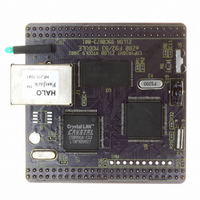
Manufacturer Part Number
EZ80F920120MOD
Description
MODULE EZ80F92 512K 20MHZ
Manufacturer
Zilog
Datasheets
1.EZ80F920120MOD.pdf
(269 pages)
2.EZ80F920120MOD.pdf
(4 pages)
3.EZ80F920120MOD.pdf
(2 pages)
Specifications of EZ80F920120MOD
Module/board Type
Development Module
Processor Series
EZ80F92x
Core
eZ80
Data Bus Width
8 bit
Program Memory Type
Flash
Program Memory Size
1 MB
Interface Type
Cable
Maximum Clock Frequency
20 MHz
Operating Supply Voltage
0 V to 3.3 V
Maximum Operating Temperature
+ 70 C
Mounting Style
SMD/SMT
Package / Case
LQFP
Development Tools By Supplier
eZ80F920200ZCOG
Minimum Operating Temperature
0 C
For Use With/related Products
eZ80F92
Lead Free Status / RoHS Status
Contains lead / RoHS non-compliant
Other names
269-3157
EZ80F920120MOD
EZ80F920120MOD


PS015308-0404
SPI Signals
The four basic SPI signals are:
•
•
•
•
These SPI signals are discussed in the following paragraphs. Each signal is described in
both MASTER and SLAVE modes.
Master In, Slave Out
The Master In, Slave Out (MISO) pin is configured as an input in a master device and as
an output in a slave device. It is one of the two lines that transfer serial data, with the most-
significant bit sent first. The MISO pin of a slave device is placed in a high-impedance
state if the slave is not selected. When the SPI is not enabled, this signal is in a high-
impedance state.
Master Out, Slave In
The Master Out, Slave In (MOSI) pin is configured as an output in a master device and as
an input in a slave device. It is one of the two lines that transfer serial data, with the most-
significant bit sent first. When the SPI is not enabled, this signal is in a high-impedance
state.
Slave Select
The active Low Slave Select (SS) input signal is used to select the SPI as a slave device. It
must be Low prior to all data communication and must stay Low for the duration of the
data transfer.
The SS input signal must be High for the SPI to operate as a master device. If the SS signal
goes Low, a Mode Fault error flag (MODF) is set in the SPI_SR register. See the SPI Sta-
tus Register (SPI_SR) on page 140 for more information.
When the Clock Phase bit (CPHA) is set to 0, the shift clock is the logical OR of SS with
SCK. In this clock phase mode, SS must go High between successive characters in an SPI
message. When CPHA is set to 1, SS can remain Low for several SPI characters. In cases
where there is only one SPI slave, its SS line could be tied Low as long as CPHA is set to
1. See the SPI Control Register (SPI_CTL) on page 139 for more information on CPHA.
Serial Clock
The Serial Clock (SCK) is used to synchronize data movement both in and out of the
device through its MOSI and MISO pins. The master and slave are each capable of
exchanging a byte of data during a sequence of eight clock cycles. Because SCK is gener-
MISO (Master In, Slave Out)
MOSI (Master Out, Slave In)
SCK (SPI Serial Clock)
SS (Slave Select)
P R E L I M I N A R Y
Product Specification
Serial Peripheral Interface
eZ80F92/eZ80F93
133
Related parts for EZ80F920120MOD
Image
Part Number
Description
Manufacturer
Datasheet
Request
R

Part Number:
Description:
Communication Controllers, ZILOG INTELLIGENT PERIPHERAL CONTROLLER (ZIP)
Manufacturer:
Zilog, Inc.
Datasheet:

Part Number:
Description:
KIT DEV FOR Z8 ENCORE 16K TO 64K
Manufacturer:
Zilog
Datasheet:

Part Number:
Description:
KIT DEV Z8 ENCORE XP 28-PIN
Manufacturer:
Zilog
Datasheet:

Part Number:
Description:
DEV KIT FOR Z8 ENCORE 8K/4K
Manufacturer:
Zilog
Datasheet:

Part Number:
Description:
KIT DEV Z8 ENCORE XP 28-PIN
Manufacturer:
Zilog
Datasheet:

Part Number:
Description:
DEV KIT FOR Z8 ENCORE 4K TO 8K
Manufacturer:
Zilog
Datasheet:
Part Number:
Description:
CMOS Z8 microcontroller. ROM 16 Kbytes, RAM 256 bytes, speed 16 MHz, 32 lines I/O, 3.0V to 5.5V
Manufacturer:
Zilog, Inc.
Datasheet:
Part Number:
Description:
Low-cost microcontroller. 512 bytes ROM, 61 bytes RAM, 8 MHz
Manufacturer:
Zilog, Inc.
Datasheet:
Part Number:
Description:
Z8 4K OTP Microcontroller
Manufacturer:
Zilog, Inc.
Datasheet:
Part Number:
Description:
CMOS SUPER8 ROMLESS MCU
Manufacturer:
Zilog, Inc.
Datasheet:
Part Number:
Description:
SL1866 CMOSZ8 OTP Microcontroller
Manufacturer:
Zilog, Inc.
Datasheet:
Part Number:
Description:
SL1866 CMOSZ8 OTP Microcontroller
Manufacturer:
Zilog, Inc.
Datasheet:
Part Number:
Description:
OTP (KB) = 1, RAM = 125, Speed = 12, I/O = 14, 8-bit Timers = 2, Comm Interfaces Other Features = Por, LV Protect, Voltage = 4.5-5.5V
Manufacturer:
Zilog, Inc.
Datasheet:
Part Number:
Description:
Manufacturer:
Zilog, Inc.
Datasheet: