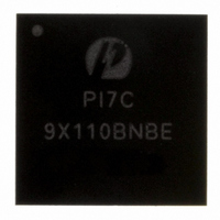
PI7C9X110BNBE Pericom Semiconductor, PI7C9X110BNBE Datasheet - Page 16

PI7C9X110BNBE
Manufacturer Part Number
PI7C9X110BNBE
Description
IC PCIE TO PCI REV BRG 160LFBGA
Manufacturer
Pericom Semiconductor
Specifications of PI7C9X110BNBE
Applications
PCI-to-PCI Bridge
Interface
I²C
Voltage - Supply
1.8 V
Package / Case
160-LBGA
Mounting Type
Surface Mount
Operating Temperature (min)
-40C
Operating Temperature Classification
Industrial
Operating Temperature (max)
85C
Rad Hardened
No
Maximum Operating Temperature
+ 85 C
Minimum Operating Temperature
- 40 C
Mounting Style
SMD/SMT
Lead Free Status / RoHS Status
Lead free / RoHS Compliant
Lead Free Status / RoHS Status
Lead free / RoHS Compliant, Compliant
Available stocks
Company
Part Number
Manufacturer
Quantity
Price
Company:
Part Number:
PI7C9X110BNBE
Manufacturer:
PLX
Quantity:
1 238
Company:
Part Number:
PI7C9X110BNBE
Manufacturer:
PERICOM31
Quantity:
193
Part Number:
PI7C9X110BNBE
Manufacturer:
PERICOM
Quantity:
20 000
2
2.1
2.2
2.3 PCI SIGNALS
Pericom Semiconductor – Confidential
PIN DEFINITIONS
SIGNAL TYPES
PCI EXPRESS SIGNALS
NAME
REFCLKP
REFCLKN
RP
RN
TP
TN
RREF
PERST_L
NAME
AD [31:0]
CBE [3:0]
PAR
FRAME_L
TYPE OF SIGNAL - DESCRIPTIONS
B
I
IU
ID
IOD
OD
O
P
G
Bi-directional
Input
Input with pull-up
Input with pull-down
Bi-directional with open drain output
Open drain output
Output
Power
Ground
PIN ASSIGNMENT
E3,
E2
G4,
H4
G1,
F1
H3
L3
PIN ASSIGNMENT
B3, A4, B4, D4, A5,
C5, D5, B6, A7, B7,
D7, A8, C8, D8, B9,
C9, C12, D14, D12,
D11, E13, F14, F13,
F11, G12, G11, H13,
H12, J14, J13, J11,
K14
C6, A10, C14, G14
B13
B10
TYPE
TYPE
O
B
B
B
B
I
I
I
I
Page 16 of 144
DESCRIPTION
Reference Clock Inputs: Connect to external 100MHz differential clock. These
signals require AC coupled with 0.1uF capacitors.
PCI Express data inputs: Differential data receiver input signals
PCI Express data outputs: Differential data transmitter output signals
Resistor Reference: It is used to connect an external resistor (2.1K Ohm +/- 1%) to
VSS to provide a reference current for the driver and equalization circuit.
PCI Express Fundamental Reset: PI7C9X110B uses this reset to initialize the
internal state machines.
DESCRIPTION
Address / Data: Multiplexed address and data bus. Address phase is aligned with
first clock of FRAME_L assertion. Data phase is aligned with IRDY_L or TRDY_L
assertion. Data is transferred on rising edges of FBCLKIN when both IRDY_L and
TRDY_L are asserted. During bus idle (both FRAME_L and IRDY_L are de-
asserted), PI7C9X110B drives AD to a valid logic level when arbiter is parking to
PI7C9X110B on PCI bus.
Command / Byte Enables (Active LOW): Multiplexed command at address phase
and byte enable at data phase. During address phase, the initiator drives commands on
CBE [3:0] signals to start the transaction. If the command is a write transaction, the
initiator will drive the byte enables during data phase. Otherwise, the target will drive
the byte enables during data phase. During bus idle, PI7C9X110B drives CBE [3:0]
signals to a valid logic level when arbiter is parking to PI7C9X110B on PCI bus.
Parity Bit: Parity bit is an even parity (i.e. even number of 1’s), which generates
based on the values of AD [31:0], CBE [3:0]. If PI7C9X110B is an initiator with a
write transaction, PI7C9X110B will tri-state PAR. If PI7C9X110B is a target and a
write transaction, PI7C9X110B will drive PAR one clock after the address or data
phase. If PI7C9X110B is a target and a read transaction, PI7C9X110B will drive
PAR one clock after the address phase and tri-state PAR during data phases. PAR is
tri-stated one cycle after the AD lines are tri-stated. During bus idle, PI7C9X110B
drives PAR to a valid logic level when arbiter is parking to PI7C9X110B on PCI bus.
FRAME (Active LOW): Driven by the initiator of a transaction to indicate the
beginning and duration an access. The de-assertion of FRAME_L indicates the final
data phase signaled by the initiator in burst transfers. Before being tri-stated, it is
driven to a de-asserted state for one cycle.
April 2010, Revision 3.0
PCIe-to-PCI Reversible Bridge
PI7C9X110


