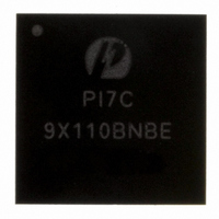
PI7C9X110BNBE Pericom Semiconductor, PI7C9X110BNBE Datasheet - Page 33

PI7C9X110BNBE
Manufacturer Part Number
PI7C9X110BNBE
Description
IC PCIE TO PCI REV BRG 160LFBGA
Manufacturer
Pericom Semiconductor
Specifications of PI7C9X110BNBE
Applications
PCI-to-PCI Bridge
Interface
I²C
Voltage - Supply
1.8 V
Package / Case
160-LBGA
Mounting Type
Surface Mount
Operating Temperature (min)
-40C
Operating Temperature Classification
Industrial
Operating Temperature (max)
85C
Rad Hardened
No
Maximum Operating Temperature
+ 85 C
Minimum Operating Temperature
- 40 C
Mounting Style
SMD/SMT
Lead Free Status / RoHS Status
Lead free / RoHS Compliant
Lead Free Status / RoHS Status
Lead free / RoHS Compliant, Compliant
Available stocks
Company
Part Number
Manufacturer
Quantity
Price
Company:
Part Number:
PI7C9X110BNBE
Manufacturer:
PLX
Quantity:
1 238
Company:
Part Number:
PI7C9X110BNBE
Manufacturer:
PERICOM31
Quantity:
193
Part Number:
PI7C9X110BNBE
Manufacturer:
PERICOM
Quantity:
20 000
7.4.1
7.4.2
7.4.3
Pericom Semiconductor – Confidential
VENDOR ID – OFFSET 00h
DEVICE ID – OFFSET 00h
COMMAND REGISTER – OFFSET 04h
RWC
RWS
RWCS
BIT
15:0
BIT
31:16
BIT
0
1
2
3
4
5
6
7
8
FUNCTION
Vendor ID
FUNCTION
Device ID
FUNCTION
I/O Space Enable
Memory Space Enable
Bus Master Enable
Special Cycle Enable
Memory Write and
Invalidate Enable
VGA Palette Snoop Enable
Parity Error Response
Enable
Wait Cycle Control
SERR_L Enable Bit
TYPE
TYPE
TYPE
RO /
RW
RW
RW
RW
RW
RW
RO
RO
RO
RO
RO
Page 33 of 144
Read/Write “1” to clear
Read/Write and Sticky
Read/Write “1” to clear and Sticky
DESCRIPTION
Identifies Pericom as the vendor of this device. Returns 12D8h when read.
DESCRIPTION
Identifies this device as the PI7C9X110. Returns E110 when read.
DESCRIPTION
0: Ignore I/O transactions on the primary interface
1: Enable response to memory transactions on the primary interface
Reset to 0
0: Ignore memory read transactions on the primary interface
1: Enable memory read transactions on the primary interface
Reset to 0
0: Do not initiate memory or I/O transactions on the primary interface and
disable response to memory and I/O transactions on the secondary interface
1: Enable the bridge to operate as a master on the primary interfaces for
memory and I/O transactions forwarded from the secondary interface. If the
primary of the reverse bridge is mode, the bridge is allowed to initiate a split
completion transaction regardless of the status bit.
Reset to 0
0: PI7C9X110 does not respond as a target to Special Cycle transactions, so
this bit is defined as Read-Only and must return 0 when read
Reset to 0
0: PI7C9X110 does not originate a Memory Write and Invalidate
transaction. Implements this bit as Read-Only and returns 0 when read
(unless forwarding a transaction for another master).
Reset to 0
This bit applies to reverse bridge only.
0: Ignore VGA palette access on the primary
1: Enable positive decoding response to VGA palette writes on the primary
interface with I/O address bits AD [9:0] equal to 3C6h, 3C8h, and 3C9h
(inclusive of ISA alias; AD [15:0] are not decoded and may be any value)
Reset to 0
0: May ignore any parity error that is detected and take its normal action
1: This bit if set, enables the setting of Master Data Parity Error bit in the
Status Register when poisoned TLP received or parity error is detected and
takes its normal action
Reset to 0
Wait cycle control not supported
Reset to 0
0: Disable
1: Enable PI7C9X110 in forward bridge mode to report non-fatal or fatal
error message to the Root Complex. Also, in reverse bridge mode to assert
SERR_L on the primary interface
April 2010, Revision 3.0
PCIe-to-PCI Reversible Bridge
PI7C9X110


