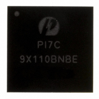
PI7C9X110BNBE Pericom Semiconductor, PI7C9X110BNBE Datasheet - Page 89

PI7C9X110BNBE
Manufacturer Part Number
PI7C9X110BNBE
Description
IC PCIE TO PCI REV BRG 160LFBGA
Manufacturer
Pericom Semiconductor
Specifications of PI7C9X110BNBE
Applications
PCI-to-PCI Bridge
Interface
I²C
Voltage - Supply
1.8 V
Package / Case
160-LBGA
Mounting Type
Surface Mount
Operating Temperature (min)
-40C
Operating Temperature Classification
Industrial
Operating Temperature (max)
85C
Rad Hardened
No
Maximum Operating Temperature
+ 85 C
Minimum Operating Temperature
- 40 C
Mounting Style
SMD/SMT
Lead Free Status / RoHS Status
Lead free / RoHS Compliant
Lead Free Status / RoHS Status
Lead free / RoHS Compliant, Compliant
Available stocks
Company
Part Number
Manufacturer
Quantity
Price
Company:
Part Number:
PI7C9X110BNBE
Manufacturer:
PLX
Quantity:
1 238
Company:
Part Number:
PI7C9X110BNBE
Manufacturer:
PERICOM31
Quantity:
193
Part Number:
PI7C9X110BNBE
Manufacturer:
PERICOM
Quantity:
20 000
7.5.36 SECONDARY CSR I/O BASE ADDRESS REGISTER – OFFSET 54h
7.5.37 UPSTREAM I/O OR MEMORY 1 BASE ADDRESS REGISTER – OFFSET 58h
7.5.38 UPSTREAM MEMORY 2 BASE ADDRESS REGISTER – OFFSET 5Ch
Pericom Semiconductor – Confidential
BIT
31:12
BIT
0
7:1
31:8
BIT
0
2:1
3
5:4
31:6
BIT
0
FUNCTION
Base Address
FUNCTION
Space Indicator
Reserved
Base Address
FUNCTION
Space Indicator
Address Type
Prefetchable control
Reserved
Base Address
FUNCTION
Space Indicator
RW/RO
RO/RW
RW/RO
TYPE
TYPE
TYPE
TYPE
RO
RO
RO
RO
RO
RO
RO
Page 89 of 144
DESCRIPTION
The size and type of this Base Address Register are defined from Upstream
Memory 0 Setup Register (Offset E4h), which can be initialized by
EEPROM (I2C) or SM Bus or Local Processor. The range of this register is
from 4KB to 2GB. The lower 4KB if this address reange map to the
PI7C9X110 CSRs into memory space. The remaining space is this range
above 4KB, if any, specifies a range for forwarding upstream memory
transactions. PI7X9X110 uses upstream Memory 0 Translated Base Register
(Offset E0h) to formulate direct address translation. If a bit in the setup
register is set to one, then the correspondent bit of this register will be
changed to RW.
Reset to 00000h
DESCRIPTION
0: Memory space
1: IO space
Reset to 1
Reset to 0
This Base Address Register maps to PI7C9X110 secondary IO space. The
maximum size is 256 bytes.
Reset to 00000000h
DESCRIPTION
0: Memory space
1: IO space
Reset to 0
00: 32-bit address decode range
01: 64-bit address decode range
10 and 11: reserved
Reset to 00
0: Memory space is non-prefetchable
1: Memory space is prefetchable
Reset to 0
Reset to 0
The size and type of this Base Address Register are defined from Upstream
IO or Memory 1 Setup Register (Offset ECh), which can be initialized by
EEPROM (I2C) or SM Bus or Local Processor. Writing a zero to bit [31] of
the setup register to disable this register. The range of this register is from
4KB to 2GB for memory space or from 64B to 256B for IO space.
PI7X9X110 uses upstream IO or Memory 1 Translated Base Register (Offset
E8h) to formulate direct address translation. If a bit in the setup register is
set to one, then the correspondent bit of this register will be changed to RW.
Reset to 00000h
DESCRIPTION
0: Memory space
1: IO space
Reset to 0
April 2010, Revision 3.0
PCIe-to-PCI Reversible Bridge
PI7C9X110


