CDB5376 Cirrus Logic Inc, CDB5376 Datasheet - Page 64
CDB5376
Manufacturer Part Number
CDB5376
Description
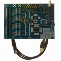
EVALUATION BOARD FOR CS5376
Manufacturer
Cirrus Logic Inc
Datasheets
1.CS5371A-ISZR.pdf
(32 pages)
2.CS4373A-ISZ.pdf
(34 pages)
3.CS5376A-IQZR.pdf
(106 pages)
4.CDB5378.pdf
(16 pages)
5.CDB5376.pdf
(80 pages)
6.CDB5376.pdf
(16 pages)
Specifications of CDB5376
Main Purpose
Seismic Evaluation System
Embedded
Yes, MCU, 8-Bit
Utilized Ic / Part
CS3301A, CS3302A, CS4373A, CS5372A, CS5376A
Primary Attributes
Quad Digital Filter
Secondary Attributes
Graphical User Interface, SPI™ & USB Interfaces
Processor To Be Evaluated
CS330x, CS4373A, CS537x
Interface Type
USB
Lead Free Status / RoHS Status
Contains lead / RoHS non-compliant
Lead Free Status / RoHS Status
Lead free / RoHS Compliant, Contains lead / RoHS non-compliant
Other names
598-1778


17.TEST BIT STREAM GENERATOR
The CS5376A test bit stream (TBS) generator cre-
ates sine wave ∆Σ bit stream data to drive an exter-
nal test DAC. The TBS digital output can also be
internally connected to the MDATA inputs for
loopback testing of the digital filter.
17.1 Pin Descriptions
TBSDATA - Pin 9
Test bit stream 1-bit ∆Σ data output.
TBSCLK - Pin 8
Test bit stream clock output. Not used by the
CS4373A test DAC.
17.2 TBS Architecture
The test bit stream generator consists of a data in-
terpolator and a digital ∆Σ modulator. It receives
periodic 24-bit data from the digital filter to create
a 1-bit ∆Σ data output on the TBSDATA pin. It also
creates a clock signal at the data rate, output to the
TBSCLK pin.
The TBS input data from the digital filter is scaled
by the TBSGAIN register (0x2B). Maximum stable
amplitude is 0x04FFFF, with 0x04B8F2 approxi-
mately full scale for the CS4373A test DAC. The
64
Figure 34. Test Bit Stream Generator Block Diagram
Digital ∆Σ Modulator
TBSGAIN Register
Digital Filter
Data Bus
TBSDATA
1-bit
24-bit
24-bit
full scale 1-bit ∆Σ output from the TBS generator is
defined as 25% minimum and 75% maximum
one’s density.
17.3 TBS Configuration
Configuration options for the TBS generator are set
through the TBSCFG register (0x2A). Gain scaling
of the TBS generator output is set by the TBSGAIN
register (0x2B).
Interpolation Factor - INTP[7:0]
Selects how many times the interpolator uses a data
point when generating the output bit stream. Inter-
polation is zero based and represents one greater
than the programmed register value.
Clock Rate - RATE[2:0]
Selects the TBSDATA and TBSCLK output rate.
Synchronization - TSYNC
Enables synchronization of the TBS output phase
to the MSYNC signal.
Clock Delay - CDLY[2:0]
Programs a fractional delay for TBSCLK with a 1/8
clock period resolution.
TBSCFG Register
Clock Generation
TBSCLK
CS5376A
DS612F4
Related parts for CDB5376
Image
Part Number
Description
Manufacturer
Datasheet
Request
R

Part Number:
Description:
Development Kit
Manufacturer:
Cirrus Logic Inc
Datasheet:
Part Number:
Description:
Development Kit
Manufacturer:
Cirrus Logic Inc
Datasheet:


Part Number:
Description:
High-efficiency PFC + Fluorescent Lamp Driver Reference Design
Manufacturer:
Cirrus Logic Inc
Datasheet:
Part Number:
Description:
Development Kit
Manufacturer:
Cirrus Logic Inc
Datasheet:
Part Number:
Description:
Development Kit
Manufacturer:
Cirrus Logic Inc
Datasheet:

Part Number:
Description:
Development Kit
Manufacturer:
Cirrus Logic Inc
Datasheet:
Part Number:
Description:
Development Kit
Manufacturer:
Cirrus Logic Inc
Datasheet:
Part Number:
Description:
Development Kit
Manufacturer:
Cirrus Logic Inc
Datasheet:
Part Number:
Description:
Development Kit
Manufacturer:
Cirrus Logic Inc
Datasheet:

Part Number:
Description:
EVALUATION BOARD FOR CS8427
Manufacturer:
Cirrus Logic Inc
Datasheet:

Part Number:
Description:
BOARD EVAL FOR CS8416 RCVR
Manufacturer:
Cirrus Logic Inc
Datasheet:

Part Number:
Description:
EVALUATION BOARD FOR CS8420
Manufacturer:
Cirrus Logic Inc
Datasheet:

Part Number:
Description:
KIT DEVELOPMENT EP9315 ARM9
Manufacturer:
Cirrus Logic Inc
Datasheet:

Part Number:
Description:
KIT DEVELOPMENT EP9302 ARM9
Manufacturer:
Cirrus Logic Inc
Datasheet: