CDB5376 Cirrus Logic Inc, CDB5376 Datasheet - Page 72
CDB5376
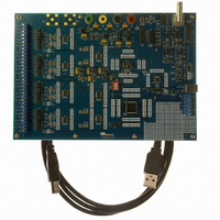
Manufacturer Part Number
CDB5376
Description
EVALUATION BOARD FOR CS5376
Manufacturer
Cirrus Logic Inc
Datasheets
1.CS5371A-ISZR.pdf
(32 pages)
2.CS4373A-ISZ.pdf
(34 pages)
3.CS5376A-IQZR.pdf
(106 pages)
4.CDB5378.pdf
(16 pages)
5.CDB5376.pdf
(80 pages)
6.CDB5376.pdf
(16 pages)
Specifications of CDB5376
Main Purpose
Seismic Evaluation System
Embedded
Yes, MCU, 8-Bit
Utilized Ic / Part
CS3301A, CS3302A, CS4373A, CS5372A, CS5376A
Primary Attributes
Quad Digital Filter
Secondary Attributes
Graphical User Interface, SPI™ & USB Interfaces
Processor To Be Evaluated
CS330x, CS4373A, CS537x
Interface Type
USB
Lead Free Status / RoHS Status
Contains lead / RoHS non-compliant
Lead Free Status / RoHS Status
Lead free / RoHS Compliant, Contains lead / RoHS non-compliant
Other names
598-1778


During a transaction, bits in SPI2CMD are output
MSB first, with data in SPI2DAT written or read
following.
20.3.3 SPI 2 Data Register
The SPI2DAT register (0x12) is a 24-bit digital fil-
ter register containing three SPI data bytes. Data in
SPI2DAT is always LSB aligned, with 1-byte data
written or received using the low byte, 2-byte data
written or received using the middle and low bytes,
and 3-byte data written or received using all three
bytes.
Data in SPI2DAT is written or read after writing
the command and address bytes from the
SPI2CMD register.
20.4 SPI 2 Transactions
The SPI 2 port operates as an SPI master to perform
write and read transactions with serial slave periph-
erals. The exact format of the SPI transactions de-
pends on the SPI mode, selected using the SCKPO
and SCKPH bits in the SPI2CTRL register.
Write Transactions
Write transactions start by writing an SPI ‘write’
(0x02) opcode and an 8-bit destination address into
the SPI2CMD register and the output data value to
the SPI2DAT register. Writing the D2SREQ bit in
the SPI2CTRL register initiates the SPI 2 transac-
tion based on the SPI2CTRL configuration.
A write transaction outputs 1 or 2 bytes from the
SPI2CMD register followed by 1, 2, or 3 bytes
from the SPI2DAT register. Write transactions are
therefore a minimum of 1 byte (DNUM = 0) and a
maximum of 5 bytes (DNUM = 4). The SPI 2 port
uses the DNUM bits in the SPI2CTRL register to
determine the total number of bytes to send during
a write transaction.
Write transactions are not required to use standard
SPI commands. If serial peripherals use non-stan-
72
dard write commands they can be written into
SPI2CMD and SPI2DAT as required.
Read Transactions
Read transactions start by writing an SPI ‘read’
(0x03) opcode and an 8-bit source address to the
SPI2CMD register. Writing the D2SREQ bit in the
SPI2CTRL register initiates the SPI 2 transaction
based on the SPI2CTRL configuration, with the
data value automatically received into the
SPI2DAT register.
A read transaction outputs 2 bytes from the
SPI2CMD register and can receive 1, 2, or 3 bytes
into the SPI2DAT register. Read transactions are a
minimum of 3 bytes (DNUM = 2) and a maximum
of 5 bytes (DNUM = 4). The SPI 2 port uses the
DNUM bits in the SPI2CTRL register to determine
the total number of bytes to send and receive during
a read transaction.
Read transactions are not required to use standard
SPI commands. If serial peripherals use non-stan-
dard read commands they can be written to the
SPI2CMD register, as long as they conform to the
format of 2 bytes out with 1, 2, or 3 bytes in.
SPI Modes
The SPI mode for the SPI 2 port is selected in the
SPI2CTRL register using the SCKPO and SCKPH
bits. The most commonly used SPI modes are
mode 0 and mode 3, both of which define the serial
clock with data valid on rising edges and transition-
ing on falling edges.
In SPI mode 0, the SCK2 serial clock is defined ini-
tially in a low state. Output data on the SO pin is
valid immediately after the chip select pin goes
low, and the first rising edge of SCK2 latches valid
data.
In SPI mode 3, the SCK2 serial clock is defined ini-
tially in a high state. Output data on the SO pin is
invalid until the initial falling edge of SCK2, and
the first rising edge of SCK2 latches valid data.
CS5376A
DS612F4
Related parts for CDB5376
Image
Part Number
Description
Manufacturer
Datasheet
Request
R

Part Number:
Description:
Development Kit
Manufacturer:
Cirrus Logic Inc
Datasheet:
Part Number:
Description:
Development Kit
Manufacturer:
Cirrus Logic Inc
Datasheet:


Part Number:
Description:
High-efficiency PFC + Fluorescent Lamp Driver Reference Design
Manufacturer:
Cirrus Logic Inc
Datasheet:
Part Number:
Description:
Development Kit
Manufacturer:
Cirrus Logic Inc
Datasheet:
Part Number:
Description:
Development Kit
Manufacturer:
Cirrus Logic Inc
Datasheet:

Part Number:
Description:
Development Kit
Manufacturer:
Cirrus Logic Inc
Datasheet:
Part Number:
Description:
Development Kit
Manufacturer:
Cirrus Logic Inc
Datasheet:
Part Number:
Description:
Development Kit
Manufacturer:
Cirrus Logic Inc
Datasheet:
Part Number:
Description:
Development Kit
Manufacturer:
Cirrus Logic Inc
Datasheet:

Part Number:
Description:
EVALUATION BOARD FOR CS8427
Manufacturer:
Cirrus Logic Inc
Datasheet:

Part Number:
Description:
BOARD EVAL FOR CS8416 RCVR
Manufacturer:
Cirrus Logic Inc
Datasheet:

Part Number:
Description:
EVALUATION BOARD FOR CS8420
Manufacturer:
Cirrus Logic Inc
Datasheet:

Part Number:
Description:
KIT DEVELOPMENT EP9315 ARM9
Manufacturer:
Cirrus Logic Inc
Datasheet:

Part Number:
Description:
KIT DEVELOPMENT EP9302 ARM9
Manufacturer:
Cirrus Logic Inc
Datasheet: