CDB5376 Cirrus Logic Inc, CDB5376 Datasheet - Page 34
CDB5376
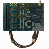
Manufacturer Part Number
CDB5376
Description
EVALUATION BOARD FOR CS5376
Manufacturer
Cirrus Logic Inc
Datasheets
1.CS5371A-ISZR.pdf
(32 pages)
2.CS4373A-ISZ.pdf
(34 pages)
3.CS5376A-IQZR.pdf
(106 pages)
4.CDB5378.pdf
(16 pages)
5.CDB5376.pdf
(80 pages)
6.CDB5376.pdf
(16 pages)
Specifications of CDB5376
Main Purpose
Seismic Evaluation System
Embedded
Yes, MCU, 8-Bit
Utilized Ic / Part
CS3301A, CS3302A, CS4373A, CS5372A, CS5376A
Primary Attributes
Quad Digital Filter
Secondary Attributes
Graphical User Interface, SPI™ & USB Interfaces
Processor To Be Evaluated
CS330x, CS4373A, CS537x
Interface Type
USB
Lead Free Status / RoHS Status
Contains lead / RoHS non-compliant
Lead Free Status / RoHS Status
Lead free / RoHS Compliant, Contains lead / RoHS non-compliant
Other names
598-1778


9.3.2 SPI 1 registers
The SPI 1 registers are shown in Figure 19 and are
24-bit registers mapped into an 8-bit register space
as high, mid, and low bytes. See “SPI 1 Registers”
on page 81 for the bit definitions of the SPI 1 reg-
isters.
9.3.3 SPI 1 transactions
A serial transaction to the SPI 1 registers starts with
an SPI opcode, followed by an address, and then
some number of data bytes written or read starting
at that address.
Typical serial write transactions require sending
groups of 5, 8, or 11 total bytes to the SPI1CMD or
SPI1DAT1 registers.
Example 5-byte write transaction to SPI1CMD
Example 5-byte write transaction to SPI1DAT1
Example 8-byte write transaction to SPI1CMD
Example 8-byte write transaction to SPI1DAT1
Example 11-byte write transaction to SPI1CMD
Typical serial read transactions require groups of 3
or 5 bytes, split between writing into MOSI and
reading from MISO.
3-byte read transaction of mid-byte of SPI1CTRL
34
02 03 12 34 56
02 06 12 34 56
02 03 12 34 56 AB CD EF
02 06 12 34 56 AB CD EF
02 03 12 34 56 AB CD EF 65 43 21
SPI1CTRL
SPI1CMD
SPI1DAT1
SPI1DAT2
Name
09 - 0B
00 - 02
03 - 05
06 - 08
Addr.
Type
R/W
R/W
R/W
R/W
# Bits
8, 8, 8
8, 8, 8
8, 8, 8
8, 8, 8
Figure 19. SPI 1 Registers
SPI 1 Control
SPI 1 Command
SPI 1 Data 1
SPI 1 Data 2
5-byte read transaction of SPI1DAT1
9.3.4 Multiple serial transactions
Some configuration commands require multiple se-
rial transactions to complete. There must be a small
delay between transactions for the CS5376A to
process the incoming data. Three methods can be
used to ensure the CS5376A is ready to receive the
next configuration command.
1) Delay a fixed 1 ms period to guarantee enough
time for the command to be completed.
2) Monitor the SINT pin for a 1 us active low pulse.
This pulse output occurs once the CS5376A com-
pletes processing the current command.
3) Verify the status of the E2DREQ bit by reading
the SPI1CTRL register. When low, the CS5376A is
ready for the next command.
9.3.5 Polling E2DREQ
One transaction type that can always be performed
no matter the delay from the previous configuration
command is reading E2DREQ in the mid-byte of
the SPI1CTRL register. A 3-byte read transaction.
MOSI: 03 01 00
MISO: xx xx 12
MOSI: 03 06 00 00 00
MISO: xx xx 12 34 56
MOSI: 03 01 00
MISO: xx xx 01 <- E2DREQ bit high
MISO: xx xx 00 <- E2DREQ bit low
Description
CS5376A
DS612F4
Related parts for CDB5376
Image
Part Number
Description
Manufacturer
Datasheet
Request
R

Part Number:
Description:
Development Kit
Manufacturer:
Cirrus Logic Inc
Datasheet:
Part Number:
Description:
Development Kit
Manufacturer:
Cirrus Logic Inc
Datasheet:


Part Number:
Description:
High-efficiency PFC + Fluorescent Lamp Driver Reference Design
Manufacturer:
Cirrus Logic Inc
Datasheet:
Part Number:
Description:
Development Kit
Manufacturer:
Cirrus Logic Inc
Datasheet:
Part Number:
Description:
Development Kit
Manufacturer:
Cirrus Logic Inc
Datasheet:

Part Number:
Description:
Development Kit
Manufacturer:
Cirrus Logic Inc
Datasheet:
Part Number:
Description:
Development Kit
Manufacturer:
Cirrus Logic Inc
Datasheet:
Part Number:
Description:
Development Kit
Manufacturer:
Cirrus Logic Inc
Datasheet:
Part Number:
Description:
Development Kit
Manufacturer:
Cirrus Logic Inc
Datasheet:

Part Number:
Description:
EVALUATION BOARD FOR CS8427
Manufacturer:
Cirrus Logic Inc
Datasheet:

Part Number:
Description:
BOARD EVAL FOR CS8416 RCVR
Manufacturer:
Cirrus Logic Inc
Datasheet:

Part Number:
Description:
EVALUATION BOARD FOR CS8420
Manufacturer:
Cirrus Logic Inc
Datasheet:

Part Number:
Description:
KIT DEVELOPMENT EP9315 ARM9
Manufacturer:
Cirrus Logic Inc
Datasheet:

Part Number:
Description:
KIT DEVELOPMENT EP9302 ARM9
Manufacturer:
Cirrus Logic Inc
Datasheet: