CDB5376 Cirrus Logic Inc, CDB5376 Datasheet - Page 97
CDB5376
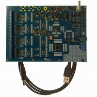
Manufacturer Part Number
CDB5376
Description
EVALUATION BOARD FOR CS5376
Manufacturer
Cirrus Logic Inc
Datasheets
1.CS5371A-ISZR.pdf
(32 pages)
2.CS4373A-ISZ.pdf
(34 pages)
3.CS5376A-IQZR.pdf
(106 pages)
4.CDB5378.pdf
(16 pages)
5.CDB5376.pdf
(80 pages)
6.CDB5376.pdf
(16 pages)
Specifications of CDB5376
Main Purpose
Seismic Evaluation System
Embedded
Yes, MCU, 8-Bit
Utilized Ic / Part
CS3301A, CS3302A, CS4373A, CS5372A, CS5376A
Primary Attributes
Quad Digital Filter
Secondary Attributes
Graphical User Interface, SPI™ & USB Interfaces
Processor To Be Evaluated
CS330x, CS4373A, CS537x
Interface Type
USB
Lead Free Status / RoHS Status
Contains lead / RoHS non-compliant
Lead Free Status / RoHS Status
Lead free / RoHS Compliant, Contains lead / RoHS non-compliant
Other names
598-1778


23.2.11 TBSCFG : 0x2A
DS612F4
Bit definitions:
23:16 INTP[7:0]
(MSB) 23
INTP7
LOOP
R/W
R/W
R/W
15
--
0
0
7
0
Figure 55. Test Bit Stream Configuration Register TBSCFG
RATE2
INTP6
RUN
R/W
R/W
R/W
22
14
0
0
6
0
Interpolation factor
0xFF: 256
0xFE: 255
...
0x01: 2
0x00: 1 (use once)
DDLY5
RATE1
INTP5
R/W
R/W
R/W
21
13
0
0
5
0
DDLY4
RATE0
INTP4
R/W
R/W
R/W
20
12
15
14:12 RATE[2:0]
11
10:8
0
0
4
0
TSYNC
--
CDLY[2:0]
TSYNC
DDLY3
INTP3
R/W
R/W
R/W
19
11
0
0
3
0
Reserved
TBSDATA and
TBSCLK output
rate.
111: 2.048 MHz
110: 1.024 MHz
101: 512 kHz
100: 256 kHz
011: 128 kHz
010: 64 kHz
001: 32 kHz
000: 4 kHz
Synchronization
1: Sync enabled
0: No sync
TBSCLK output
phase delay
111: 7/8 period
110: 3/4 period
101: 5/8 period
100: 1/2 period
011: 3/8 period
010: 1/4 period
001: 1/8 period
000: none
CDLY2
DDLY2
INTP2
R/W
R/W
R/W
18
10
0
0
2
0
CDLY1
DDLY1
INTP1
R/W
R/W
R/W
17
0
9
0
1
0
7
6
5:0
(LSB) 0
DDLY0
RUN
DDLY[5:0]
CDLY0
LOOP
INTP0
R/W
R/W
R/W
16
0
8
0
0
Loopback
TBSDATA output
to MDATA inputs
1: Enabled
0: Disabled
Run Test Bit Stream
1: Enabled
0: Disabled
TBSDATA output
delay
0x3F: 63 bits
0x3E: 62 bits
...
0x01: 1 bit
0x00: 0 bits ( no
delay)
DF Address: 0x2A
--
R
W
R/W
Bits in bottom rows
are reset condition
Not defined;
read as 0
Readable
Writable
Readable and
Writable
CS5376A
97
Related parts for CDB5376
Image
Part Number
Description
Manufacturer
Datasheet
Request
R

Part Number:
Description:
Development Kit
Manufacturer:
Cirrus Logic Inc
Datasheet:
Part Number:
Description:
Development Kit
Manufacturer:
Cirrus Logic Inc
Datasheet:


Part Number:
Description:
High-efficiency PFC + Fluorescent Lamp Driver Reference Design
Manufacturer:
Cirrus Logic Inc
Datasheet:
Part Number:
Description:
Development Kit
Manufacturer:
Cirrus Logic Inc
Datasheet:
Part Number:
Description:
Development Kit
Manufacturer:
Cirrus Logic Inc
Datasheet:

Part Number:
Description:
Development Kit
Manufacturer:
Cirrus Logic Inc
Datasheet:
Part Number:
Description:
Development Kit
Manufacturer:
Cirrus Logic Inc
Datasheet:
Part Number:
Description:
Development Kit
Manufacturer:
Cirrus Logic Inc
Datasheet:
Part Number:
Description:
Development Kit
Manufacturer:
Cirrus Logic Inc
Datasheet:

Part Number:
Description:
EVALUATION BOARD FOR CS8427
Manufacturer:
Cirrus Logic Inc
Datasheet:

Part Number:
Description:
BOARD EVAL FOR CS8416 RCVR
Manufacturer:
Cirrus Logic Inc
Datasheet:

Part Number:
Description:
EVALUATION BOARD FOR CS8420
Manufacturer:
Cirrus Logic Inc
Datasheet:

Part Number:
Description:
KIT DEVELOPMENT EP9315 ARM9
Manufacturer:
Cirrus Logic Inc
Datasheet:

Part Number:
Description:
KIT DEVELOPMENT EP9302 ARM9
Manufacturer:
Cirrus Logic Inc
Datasheet: