CDB5376 Cirrus Logic Inc, CDB5376 Datasheet - Page 39
CDB5376
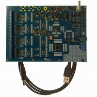
Manufacturer Part Number
CDB5376
Description
EVALUATION BOARD FOR CS5376
Manufacturer
Cirrus Logic Inc
Datasheets
1.CS5371A-ISZR.pdf
(32 pages)
2.CS4373A-ISZ.pdf
(34 pages)
3.CS5376A-IQZR.pdf
(106 pages)
4.CDB5378.pdf
(16 pages)
5.CDB5376.pdf
(80 pages)
6.CDB5376.pdf
(16 pages)
Specifications of CDB5376
Main Purpose
Seismic Evaluation System
Embedded
Yes, MCU, 8-Bit
Utilized Ic / Part
CS3301A, CS3302A, CS4373A, CS5372A, CS5376A
Primary Attributes
Quad Digital Filter
Secondary Attributes
Graphical User Interface, SPI™ & USB Interfaces
Processor To Be Evaluated
CS330x, CS4373A, CS537x
Interface Type
USB
Lead Free Status / RoHS Status
Contains lead / RoHS non-compliant
Lead Free Status / RoHS Status
Lead free / RoHS Compliant, Contains lead / RoHS non-compliant
Other names
598-1778


10.MODULATOR INTERFACE
The CS5376A performs digital filtering for up to
four ∆Σ modulators. Signals from the modulators
are connected through the modulator data interface
(MDI).
10.1 Pin Descriptions
MCLK, MCLK/2 - Pins 13, 12
Modulator clock outputs. Nominally 2.048 MHz
and 1.024 MHz.
MSYNC - Pin 14
Modulator synchronization signal output. Generat-
ed from the SYNC input.
MDATA1 - MDATA4 - Pins 15, 17, 19, 21
Modulator data inputs, nominally 512 kbit/s.
MFLAG1 - MFLAG4 - Pins 16, 18, 20, 22
Modulator flag inputs. Driven high when modula-
tor is unstable due to an analog over-range signal.
DS612F4
MCLK
MCLK/2
MSYNC
MDATA[4:1]
MFLAG[4:1]
Correction
DC Offset
& Gain
MDI Input
MCLK /
MSYNC
Generate
512 kHz
Figure 20. Modulator Data Interface
CLK
SYNC
Output to High Speed Serial Data Port (SD Port)
SINC
Filter
Output Rate 4000 SPS ~ 1 SPS
10.2 Modulator Clock Generation
The MCLK and MCLK/2 outputs are low-jitter,
low-skew modulator clocks generated from the
32.768 MHz master clock.
MCLK typically operates at 2.048 MHz unless an-
alog low-power modes require a 1.024 MHz mod-
ulator clock. MCLK/2 always produces a clock at
half the selected MCLK rate.
The MCLK rate is selected and the MCLK and
MCLK/2 outputs are enabled by bits in the digital
filter CONFIG register (0x00). By default MCLK
and MCLK/2 are disabled and driven low.
10.3 Modulator Synchronization
The MSYNC output signal follows an input on the
SYNC pin. MSYNC phase aligns the modulator
sampling instant to guarantee synchronous analog
sampling across a measurement network.
MSYNC is enabled by a bit in the CONFIG register
(0x00). By default SYNC inputs do not cause an
MSYNC output.
FIR
Filters
IIR
Filter
CS5376A
39
Related parts for CDB5376
Image
Part Number
Description
Manufacturer
Datasheet
Request
R

Part Number:
Description:
Development Kit
Manufacturer:
Cirrus Logic Inc
Datasheet:
Part Number:
Description:
Development Kit
Manufacturer:
Cirrus Logic Inc
Datasheet:


Part Number:
Description:
High-efficiency PFC + Fluorescent Lamp Driver Reference Design
Manufacturer:
Cirrus Logic Inc
Datasheet:
Part Number:
Description:
Development Kit
Manufacturer:
Cirrus Logic Inc
Datasheet:
Part Number:
Description:
Development Kit
Manufacturer:
Cirrus Logic Inc
Datasheet:

Part Number:
Description:
Development Kit
Manufacturer:
Cirrus Logic Inc
Datasheet:
Part Number:
Description:
Development Kit
Manufacturer:
Cirrus Logic Inc
Datasheet:
Part Number:
Description:
Development Kit
Manufacturer:
Cirrus Logic Inc
Datasheet:
Part Number:
Description:
Development Kit
Manufacturer:
Cirrus Logic Inc
Datasheet:

Part Number:
Description:
EVALUATION BOARD FOR CS8427
Manufacturer:
Cirrus Logic Inc
Datasheet:

Part Number:
Description:
BOARD EVAL FOR CS8416 RCVR
Manufacturer:
Cirrus Logic Inc
Datasheet:

Part Number:
Description:
EVALUATION BOARD FOR CS8420
Manufacturer:
Cirrus Logic Inc
Datasheet:

Part Number:
Description:
KIT DEVELOPMENT EP9315 ARM9
Manufacturer:
Cirrus Logic Inc
Datasheet:

Part Number:
Description:
KIT DEVELOPMENT EP9302 ARM9
Manufacturer:
Cirrus Logic Inc
Datasheet: