CDB5376 Cirrus Logic Inc, CDB5376 Datasheet - Page 61
CDB5376
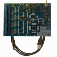
Manufacturer Part Number
CDB5376
Description
EVALUATION BOARD FOR CS5376
Manufacturer
Cirrus Logic Inc
Datasheets
1.CS5371A-ISZR.pdf
(32 pages)
2.CS4373A-ISZ.pdf
(34 pages)
3.CS5376A-IQZR.pdf
(106 pages)
4.CDB5378.pdf
(16 pages)
5.CDB5376.pdf
(80 pages)
6.CDB5376.pdf
(16 pages)
Specifications of CDB5376
Main Purpose
Seismic Evaluation System
Embedded
Yes, MCU, 8-Bit
Utilized Ic / Part
CS3301A, CS3302A, CS4373A, CS5372A, CS5376A
Primary Attributes
Quad Digital Filter
Secondary Attributes
Graphical User Interface, SPI™ & USB Interfaces
Processor To Be Evaluated
CS330x, CS4373A, CS537x
Interface Type
USB
Lead Free Status / RoHS Status
Contains lead / RoHS non-compliant
Lead Free Status / RoHS Status
Lead free / RoHS Compliant, Contains lead / RoHS non-compliant
Other names
598-1778


16.SERIAL DATA PORT
Once digital filtering is complete, each 24-bit out-
put sample is combined with an 8-bit status byte.
These 32-bit data words are written to an 8-deep
FIFO buffer and then transmitted to the communi-
cations channel through a high speed serial data
port (SD port).
16.1 Pin Descriptions
SDTKI - Pin 64
Token input, requests an SD port transaction.
SDRDY - Pin 61
Data ready output signal, active low. Open drain
output requiring a 10 kΩ pull-up resistor.
SDCLK - Pin 62
Serial clock input.
SDDAT - Pin 60
Serial data output. Data valid on rising edge of
SDCLK, transition on falling edge.
SDTKO - Pin 63
Token output, ends an SD port transaction. Passes
through the SDTKI signal when no data is available
in the SD port output FIFO.
DS612F4
System Telemetry
Data Ready
Token Out
Clock Out
Token In
Data In
Figure 31. Serial Data Port Block Diagram
16.2 SD Port Data Format
Serial data transactions transfer 32-bit words. Each
word consists of an 8-bit status byte followed by a
24-bit output sample. The status byte, shown in
Figure 32, has an MFLAG bit, channel bits, a time
break bit, and a FIFO overflow bit.
MFLAG Bit - MFLAG
The MFLAG bit is set when an MFLAG signal is
received on the MFLAG1-MFLAG4 pins. When
received, that channel MFLAG bit is set in the next
output word. See “Modulator Interface” on page 39
for more information about MFLAG.
Channel Bits - CH[1:0]
Channel bits indicate from which conversion chan-
nel the data word is from. The channel number,
CH[1:0], is zero based.
Time Break Bit - TB
The time break bit marks a timing reference based
on a rising edge into the TIMEB pin. After a pro-
grammed delay, the TB bit in the status byte is set
for one output sample in all channels. The TIME-
CH[1:0] = 00 = Channel 1
CH[1:0] = 01 = Channel 2
CH[1:0] = 10 = Channel 3
CH[1:0] = 11 = Channel 4
SDTKI
SDRDY
SDDAT
SDTKO
SDCLK
CS5376A
CS5376A
61
Related parts for CDB5376
Image
Part Number
Description
Manufacturer
Datasheet
Request
R

Part Number:
Description:
Development Kit
Manufacturer:
Cirrus Logic Inc
Datasheet:
Part Number:
Description:
Development Kit
Manufacturer:
Cirrus Logic Inc
Datasheet:


Part Number:
Description:
High-efficiency PFC + Fluorescent Lamp Driver Reference Design
Manufacturer:
Cirrus Logic Inc
Datasheet:
Part Number:
Description:
Development Kit
Manufacturer:
Cirrus Logic Inc
Datasheet:
Part Number:
Description:
Development Kit
Manufacturer:
Cirrus Logic Inc
Datasheet:

Part Number:
Description:
Development Kit
Manufacturer:
Cirrus Logic Inc
Datasheet:
Part Number:
Description:
Development Kit
Manufacturer:
Cirrus Logic Inc
Datasheet:
Part Number:
Description:
Development Kit
Manufacturer:
Cirrus Logic Inc
Datasheet:
Part Number:
Description:
Development Kit
Manufacturer:
Cirrus Logic Inc
Datasheet:

Part Number:
Description:
EVALUATION BOARD FOR CS8427
Manufacturer:
Cirrus Logic Inc
Datasheet:

Part Number:
Description:
BOARD EVAL FOR CS8416 RCVR
Manufacturer:
Cirrus Logic Inc
Datasheet:

Part Number:
Description:
EVALUATION BOARD FOR CS8420
Manufacturer:
Cirrus Logic Inc
Datasheet:

Part Number:
Description:
KIT DEVELOPMENT EP9315 ARM9
Manufacturer:
Cirrus Logic Inc
Datasheet:

Part Number:
Description:
KIT DEVELOPMENT EP9302 ARM9
Manufacturer:
Cirrus Logic Inc
Datasheet: