CDB5376 Cirrus Logic Inc, CDB5376 Datasheet - Page 67
CDB5376
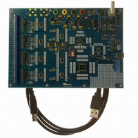
Manufacturer Part Number
CDB5376
Description
EVALUATION BOARD FOR CS5376
Manufacturer
Cirrus Logic Inc
Datasheets
1.CS5371A-ISZR.pdf
(32 pages)
2.CS4373A-ISZ.pdf
(34 pages)
3.CS5376A-IQZR.pdf
(106 pages)
4.CDB5378.pdf
(16 pages)
5.CDB5376.pdf
(80 pages)
6.CDB5376.pdf
(16 pages)
Specifications of CDB5376
Main Purpose
Seismic Evaluation System
Embedded
Yes, MCU, 8-Bit
Utilized Ic / Part
CS3301A, CS3302A, CS4373A, CS5372A, CS5376A
Primary Attributes
Quad Digital Filter
Secondary Attributes
Graphical User Interface, SPI™ & USB Interfaces
Processor To Be Evaluated
CS330x, CS4373A, CS537x
Interface Type
USB
Lead Free Status / RoHS Status
Contains lead / RoHS non-compliant
Lead Free Status / RoHS Status
Lead free / RoHS Compliant, Contains lead / RoHS non-compliant
Other names
598-1778


18.TIME BREAK CONTROLLER
A time break signal is used to mark timing events
that occur during measurement. An external signal
sets a flag in the status byte of an output sample to
mark when the external event occurred.
A rising edge input to the TIMEB pin causes the
TB timing reference flag to be set in the SD port
status byte. When set, the TB flag appears for only
one output sample in the status byte of all enabled
channels. The TB flag output can be delayed by
programming a sample delay value into the TIME-
BRK digital filter register.
18.1 Pin Description
TIMEB - Pin 57
Time break input pin, rising edge triggered.
18.2 Time Break Operation
An externally generated timing reference signal ap-
plied to the TIMEB pin initiates an internal sample
counter. After a number of output samples have
passed, programmed in the TIMEBRK digital filter
register (0x29), the TB flag is set in the status byte
of the SD port output word for all enabled channels.
The TB flag is automatically cleared for subse-
quent data words, and appears for only one output
sample in each channel.
DS612F4
TIMEB
Figure 35. Time Break Block Diagram
Delay Counter
TIMEBRK
18.3 Time Break Delay
The TIMEBRK register (0x29) sets a sample delay
between a received rising edge on the TIMEB pin
and writing the TB flag into the SD port status byte.
The programmable sample counter can compensate
for group delay through the digital filters. When the
proper group delay value is programmed into the
TIMEBRK register, the TB flag will be set in the
status byte of the measurement sample taken when
the timing reference signal was received.
18.3.1 Step Input and Group Delay
A simple method to empirically measure the step
response and group delay of a CS5376A measure-
ment channel is to use the time break signal as both
a timing reference input and an analog step input.
When a rising edge is received on the TIMEB pin
with no delay programmed into the TIMEBRK reg-
ister, the TB flag is set in the next SD port status
byte. The same rising edge can act as a step input to
the analog channel, propagating through the digital
filter to appear as a rising edge in the measurement
data. By comparing the timing of the TB status flag
output and the rising edge in the measurement data,
the measurement channel group delay can be deter-
mined.
Status Byte
in SD Port
TB Flag
CS5376A
67
Related parts for CDB5376
Image
Part Number
Description
Manufacturer
Datasheet
Request
R

Part Number:
Description:
Development Kit
Manufacturer:
Cirrus Logic Inc
Datasheet:
Part Number:
Description:
Development Kit
Manufacturer:
Cirrus Logic Inc
Datasheet:


Part Number:
Description:
High-efficiency PFC + Fluorescent Lamp Driver Reference Design
Manufacturer:
Cirrus Logic Inc
Datasheet:
Part Number:
Description:
Development Kit
Manufacturer:
Cirrus Logic Inc
Datasheet:
Part Number:
Description:
Development Kit
Manufacturer:
Cirrus Logic Inc
Datasheet:

Part Number:
Description:
Development Kit
Manufacturer:
Cirrus Logic Inc
Datasheet:
Part Number:
Description:
Development Kit
Manufacturer:
Cirrus Logic Inc
Datasheet:
Part Number:
Description:
Development Kit
Manufacturer:
Cirrus Logic Inc
Datasheet:
Part Number:
Description:
Development Kit
Manufacturer:
Cirrus Logic Inc
Datasheet:

Part Number:
Description:
EVALUATION BOARD FOR CS8427
Manufacturer:
Cirrus Logic Inc
Datasheet:

Part Number:
Description:
BOARD EVAL FOR CS8416 RCVR
Manufacturer:
Cirrus Logic Inc
Datasheet:

Part Number:
Description:
EVALUATION BOARD FOR CS8420
Manufacturer:
Cirrus Logic Inc
Datasheet:

Part Number:
Description:
KIT DEVELOPMENT EP9315 ARM9
Manufacturer:
Cirrus Logic Inc
Datasheet:

Part Number:
Description:
KIT DEVELOPMENT EP9302 ARM9
Manufacturer:
Cirrus Logic Inc
Datasheet: