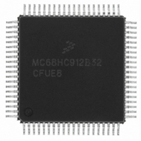
MCHC912B32CFUE8 Freescale Semiconductor, MCHC912B32CFUE8 Datasheet - Page 109

MCHC912B32CFUE8
Manufacturer Part Number
MCHC912B32CFUE8
Description
IC MCU 32K FLASH 8MHZ 80-QFP
Manufacturer
Freescale Semiconductor
Series
HC12r
Datasheet
1.MCHC912B32CFUE8.pdf
(334 pages)
Specifications of MCHC912B32CFUE8
Core Processor
CPU12
Core Size
16-Bit
Speed
8MHz
Connectivity
SCI, SPI
Peripherals
POR, PWM, WDT
Number Of I /o
63
Program Memory Size
32KB (32K x 8)
Program Memory Type
FLASH
Eeprom Size
768 x 8
Ram Size
1K x 8
Voltage - Supply (vcc/vdd)
4.5 V ~ 5.5 V
Data Converters
A/D 8x10b
Oscillator Type
External
Operating Temperature
-40°C ~ 85°C
Package / Case
80-QFP
Cpu Family
HC12
Device Core Size
16b
Frequency (max)
8MHz
Interface Type
SCI/SPI
Total Internal Ram Size
1KB
# I/os (max)
63
Operating Supply Voltage (typ)
5V
Operating Supply Voltage (max)
5.5V
Operating Supply Voltage (min)
4.5V
On-chip Adc
8-chx10-bit
Instruction Set Architecture
CISC
Operating Temp Range
-40C to 85C
Operating Temperature Classification
Industrial
Mounting
Surface Mount
Pin Count
80
Package Type
PQFP
Package
80PQFP
Family Name
HC12
Maximum Speed
8 MHz
Operating Supply Voltage
5 V
Data Bus Width
16 Bit
Number Of Programmable I/os
63
Processor Series
HC912B
Core
HC12
Data Ram Size
1 KB
Maximum Clock Frequency
8 MHz
Maximum Operating Temperature
+ 85 C
Mounting Style
SMD/SMT
3rd Party Development Tools
EWHCS12
Development Tools By Supplier
M68EVB912B32E
Minimum Operating Temperature
- 40 C
Lead Free Status / RoHS Status
Lead free / RoHS Compliant
Available stocks
Company
Part Number
Manufacturer
Quantity
Price
Company:
Part Number:
MCHC912B32CFUE8
Manufacturer:
Freescale Semiconductor
Quantity:
10 000
- Current page: 109 of 334
- Download datasheet (2Mb)
8.7 Program/Erase Protection Interlocks
The FLASH EEPROM program and erase mechanisms provide maximum protection from accidental
programming or erasure.
The voltage required to program/erase the FLASH EEPROM (V
is not present, no programming/erasing will occur. Furthermore, the program/erase voltage will not be
applied to the FLASH EEPROM unless turned on by setting a control bit (ENPE). The ENPE bit may not
be set unless the programming address and data latches have been written previously with a valid
address. The latches may not be written unless enabled by setting a control bit (LAT). The LAT and ENPE
control bits must be written on separate writes to the control register (FEECTL) and must be separated
by a write to the programming latches. The ERAS and LAT bits are also protected when ENPE is set. This
prevents inadvertent switching between erase/program mode and also prevents the latched data and
address from being changed after a program cycle has been initiated.
8.8 Stop or Wait Mode
When STOP or WAIT commands are executed, the MCU puts the FLASH EEPROM in stop or wait mode.
In these modes, the FLASH module will cease erasure or programming immediately.
8.9 Test Mode
The FLASH EEPROM has some special test functions which are only accessible when the device is in
test mode. Test mode is indicated to the FLASH EEPROM module when the SMOD line on the LIB is
asserted. When SMOD is asserted, the special test control bits may be accessed via the LIB to invoke
the special test functions in the FLASH EEPROM module. When SMOD is not asserted, writes to the test
control bits have no effect and all bits in the test register FEETST will be cleared. This ensures that FLASH
EEPROM test mode cannot be invoked inadvertently during normal operation.
The FLASH EEPROM module will operate normally, even if SMOD is asserted, until a special test function
is invoked. The test mode adds additional features over normal mode. These features allow the tests to
be performed even after the device is installed in the final product.
Freescale Semiconductor
It is advised to not enter stop or wait modes when programming the FLASH
array. The FLASH EEPROM module is not able to recover from stop mode
without a 250-ns delay. If the operating bus frequency is greater than 4
MHz, the DLY bit must be set to1 to use the FLASH after recovering from
stop mode. Other options are to map the EEPROM module over the FLASH
module in the memory map with DLY = 0 and place the interrupt vectors in
the EEPROM array or use reset to recover from a stop mode executed from
FLASH EEPROM. Recovery from a STOP instruction executed from
EEPROM and RAM operates normally.
M68HC12B Family Data Sheet, Rev. 9.1
NOTE
FP
) is supplied via an external pin. If V
Program/Erase Protection Interlocks
109
FP
Related parts for MCHC912B32CFUE8
Image
Part Number
Description
Manufacturer
Datasheet
Request
R
Part Number:
Description:
Manufacturer:
Freescale Semiconductor, Inc
Datasheet:
Part Number:
Description:
Manufacturer:
Freescale Semiconductor, Inc
Datasheet:
Part Number:
Description:
Manufacturer:
Freescale Semiconductor, Inc
Datasheet:
Part Number:
Description:
Manufacturer:
Freescale Semiconductor, Inc
Datasheet:
Part Number:
Description:
Manufacturer:
Freescale Semiconductor, Inc
Datasheet:
Part Number:
Description:
Manufacturer:
Freescale Semiconductor, Inc
Datasheet:
Part Number:
Description:
Manufacturer:
Freescale Semiconductor, Inc
Datasheet:
Part Number:
Description:
Manufacturer:
Freescale Semiconductor, Inc
Datasheet:
Part Number:
Description:
Manufacturer:
Freescale Semiconductor, Inc
Datasheet:
Part Number:
Description:
Manufacturer:
Freescale Semiconductor, Inc
Datasheet:
Part Number:
Description:
Manufacturer:
Freescale Semiconductor, Inc
Datasheet:
Part Number:
Description:
Manufacturer:
Freescale Semiconductor, Inc
Datasheet:
Part Number:
Description:
Manufacturer:
Freescale Semiconductor, Inc
Datasheet:
Part Number:
Description:
Manufacturer:
Freescale Semiconductor, Inc
Datasheet:
Part Number:
Description:
Manufacturer:
Freescale Semiconductor, Inc
Datasheet:


