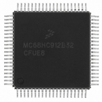
MCHC912B32CFUE8 Freescale Semiconductor, MCHC912B32CFUE8 Datasheet - Page 281

MCHC912B32CFUE8
Manufacturer Part Number
MCHC912B32CFUE8
Description
IC MCU 32K FLASH 8MHZ 80-QFP
Manufacturer
Freescale Semiconductor
Series
HC12r
Datasheet
1.MCHC912B32CFUE8.pdf
(334 pages)
Specifications of MCHC912B32CFUE8
Core Processor
CPU12
Core Size
16-Bit
Speed
8MHz
Connectivity
SCI, SPI
Peripherals
POR, PWM, WDT
Number Of I /o
63
Program Memory Size
32KB (32K x 8)
Program Memory Type
FLASH
Eeprom Size
768 x 8
Ram Size
1K x 8
Voltage - Supply (vcc/vdd)
4.5 V ~ 5.5 V
Data Converters
A/D 8x10b
Oscillator Type
External
Operating Temperature
-40°C ~ 85°C
Package / Case
80-QFP
Cpu Family
HC12
Device Core Size
16b
Frequency (max)
8MHz
Interface Type
SCI/SPI
Total Internal Ram Size
1KB
# I/os (max)
63
Operating Supply Voltage (typ)
5V
Operating Supply Voltage (max)
5.5V
Operating Supply Voltage (min)
4.5V
On-chip Adc
8-chx10-bit
Instruction Set Architecture
CISC
Operating Temp Range
-40C to 85C
Operating Temperature Classification
Industrial
Mounting
Surface Mount
Pin Count
80
Package Type
PQFP
Package
80PQFP
Family Name
HC12
Maximum Speed
8 MHz
Operating Supply Voltage
5 V
Data Bus Width
16 Bit
Number Of Programmable I/os
63
Processor Series
HC912B
Core
HC12
Data Ram Size
1 KB
Maximum Clock Frequency
8 MHz
Maximum Operating Temperature
+ 85 C
Mounting Style
SMD/SMT
3rd Party Development Tools
EWHCS12
Development Tools By Supplier
M68EVB912B32E
Minimum Operating Temperature
- 40 C
Lead Free Status / RoHS Status
Lead free / RoHS Compliant
Available stocks
Company
Part Number
Manufacturer
Quantity
Price
Company:
Part Number:
MCHC912B32CFUE8
Manufacturer:
Freescale Semiconductor
Quantity:
10 000
- Current page: 281 of 334
- Download datasheet (2Mb)
FRZ1 and FRZ0 — Background Debug (Freeze) Enable Bits
17.3.5 ATD Control Register 4
The ATD control register 4 (ATDCTL4) selects the clock source and sets up the prescaler. Writes to the
ATD control registers initiate a new conversion sequence. If a write occurs while a conversion is in
progress, the conversion is aborted and ATD activity halts until a write to ATDCTL5 occurs.
S10BM — ATD 10-Bit Mode Control Bit
SMP1 and SMP0 — Select Sample Time Bits
PRS4–PRS0 — Select Divide-By Factor for ATD P-Clock Prescaler Bits
Freescale Semiconductor
When debugging an application, it is useful in many cases to have the ATD pause when a breakpoint
is encountered. These two bits determine how the ATD will respond when background debug mode
becomes active. See
These bits are used to select one of four sample times after the buffered sample and transfer has
occurred. See
The binary value written to these bits (1 to 31) selects the divide-by factor for the modulo counter-based
prescaler. The P clock is divided by this value plus one, and then fed into a divide-by-two circuit to
generate the ATD module clock. The divide-by-two circuit ensures symmetry of the output clock signal.
0 = 8-bit operation
1 = 10-bit operation
SMP1
Address: $0064
Reset:
Read:
0
0
1
1
Write:
FRZ1
Table
0
0
1
1
SMP0
Table 17-1. ATD Response to Background Debug Enable
S10BM
0
1
0
1
Bit 7
17-2.
Table
0
FRZ0
Figure 17-6. ATD Control Register 4 (ATDCTL4)
0
1
0
1
16 ATD clock periods
2 ATD clock periods
4 ATD clock periods
8 ATD clock periods
Table 17-2. Final Sample Time Selection
17-1.
SMP1
Sample Time
6
0
Continue conversions in active background mode
Reserved
Finish current conversion, then freeze
Freeze when BDM is active
M68HC12B Family Data Sheet, Rev. 9.1
Final
SMP0
5
0
PRS4
18 ATD clock periods
20 ATD clock periods
24 ATD clock periods
32 ATD clock periods
4
0
Conversion Time
ATD Response
Total 8-Bit
PRS3
3
0
PRS2
2
0
20 ATD clock periods
22 ATD clock periods
26 ATD clock periods
34 ATD clock periods
Conversion Time
Total 10-Bit
PRS1
1
0
PRS0
Bit 0
1
ATD Registers
281
Related parts for MCHC912B32CFUE8
Image
Part Number
Description
Manufacturer
Datasheet
Request
R
Part Number:
Description:
Manufacturer:
Freescale Semiconductor, Inc
Datasheet:
Part Number:
Description:
Manufacturer:
Freescale Semiconductor, Inc
Datasheet:
Part Number:
Description:
Manufacturer:
Freescale Semiconductor, Inc
Datasheet:
Part Number:
Description:
Manufacturer:
Freescale Semiconductor, Inc
Datasheet:
Part Number:
Description:
Manufacturer:
Freescale Semiconductor, Inc
Datasheet:
Part Number:
Description:
Manufacturer:
Freescale Semiconductor, Inc
Datasheet:
Part Number:
Description:
Manufacturer:
Freescale Semiconductor, Inc
Datasheet:
Part Number:
Description:
Manufacturer:
Freescale Semiconductor, Inc
Datasheet:
Part Number:
Description:
Manufacturer:
Freescale Semiconductor, Inc
Datasheet:
Part Number:
Description:
Manufacturer:
Freescale Semiconductor, Inc
Datasheet:
Part Number:
Description:
Manufacturer:
Freescale Semiconductor, Inc
Datasheet:
Part Number:
Description:
Manufacturer:
Freescale Semiconductor, Inc
Datasheet:
Part Number:
Description:
Manufacturer:
Freescale Semiconductor, Inc
Datasheet:
Part Number:
Description:
Manufacturer:
Freescale Semiconductor, Inc
Datasheet:
Part Number:
Description:
Manufacturer:
Freescale Semiconductor, Inc
Datasheet:


