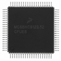
MCHC912B32CFUE8 Freescale Semiconductor, MCHC912B32CFUE8 Datasheet - Page 34

MCHC912B32CFUE8
Manufacturer Part Number
MCHC912B32CFUE8
Description
IC MCU 32K FLASH 8MHZ 80-QFP
Manufacturer
Freescale Semiconductor
Series
HC12r
Datasheet
1.MCHC912B32CFUE8.pdf
(334 pages)
Specifications of MCHC912B32CFUE8
Core Processor
CPU12
Core Size
16-Bit
Speed
8MHz
Connectivity
SCI, SPI
Peripherals
POR, PWM, WDT
Number Of I /o
63
Program Memory Size
32KB (32K x 8)
Program Memory Type
FLASH
Eeprom Size
768 x 8
Ram Size
1K x 8
Voltage - Supply (vcc/vdd)
4.5 V ~ 5.5 V
Data Converters
A/D 8x10b
Oscillator Type
External
Operating Temperature
-40°C ~ 85°C
Package / Case
80-QFP
Cpu Family
HC12
Device Core Size
16b
Frequency (max)
8MHz
Interface Type
SCI/SPI
Total Internal Ram Size
1KB
# I/os (max)
63
Operating Supply Voltage (typ)
5V
Operating Supply Voltage (max)
5.5V
Operating Supply Voltage (min)
4.5V
On-chip Adc
8-chx10-bit
Instruction Set Architecture
CISC
Operating Temp Range
-40C to 85C
Operating Temperature Classification
Industrial
Mounting
Surface Mount
Pin Count
80
Package Type
PQFP
Package
80PQFP
Family Name
HC12
Maximum Speed
8 MHz
Operating Supply Voltage
5 V
Data Bus Width
16 Bit
Number Of Programmable I/os
63
Processor Series
HC912B
Core
HC12
Data Ram Size
1 KB
Maximum Clock Frequency
8 MHz
Maximum Operating Temperature
+ 85 C
Mounting Style
SMD/SMT
3rd Party Development Tools
EWHCS12
Development Tools By Supplier
M68EVB912B32E
Minimum Operating Temperature
- 40 C
Lead Free Status / RoHS Status
Lead free / RoHS Compliant
Available stocks
Company
Part Number
Manufacturer
Quantity
Price
Company:
Part Number:
MCHC912B32CFUE8
Manufacturer:
Freescale Semiconductor
Quantity:
10 000
- Current page: 34 of 334
- Download datasheet (2Mb)
General Description
1.6.4.4 Port DLC
The MC68HC912B32 and MC68HC12BE32 contain the port DLC.
Byte data link communications (BDLC) pins can be configured as general-purpose I/O port DLC. When
BDLC functions are not enabled, the port has seven general-purpose I/O pins, PDLC6–PDLC0. The port
DLC control register (DLCSCR) controls port DLC function. The BDLC function, enabled with the
BDLCEN bit, takes precedence over other port functions.
The port DLC data direction register (DDRDLC) determines whether each port DLC pin is an input or
output. Setting a bit in DDRDLC makes the corresponding pin in port DLC an output; clearing a bit makes
the corresponding pin an input. After reset, port DLC pins are configured as inputs.
When the PUPDLC bit in the DLCSCR register is set, all port DLC input pins are pulled up internally by
an active pullup device.
Setting the RDPDLC bit in register DLCSCR causes all port DLC outputs to have reduced drive level.
Levels are at normal drive capability after reset. RDPDLC can be written anytime after reset. Refer to
Chapter 15 Byte Data Link Communications
(BDLC).
1.6.4.5 Port CAN
The MC68HC(9)12BC32 contains the port CAN.
The port CAN has five general-purpose I/O pins, PCAN[6:2]. The msCAN12 receive pin, RxCAN, and
transmit pin, TxCAN, cannot be configured as general-purpose I/O on port CAN.
The msCAN data direction register (DDRCAN) determines whether each port CAN pin PCAN[6:2] is an
input or output. Setting a bit in DDRCAN makes the corresponding pin in port CAN an output; clearing a
bit makes the corresponding pin an input. After reset, port CAN pins PCAN[6:2] are configured as inputs.
When a read to the port CAN is performed, the value read from the most significant bit (MSB) depends
on the MSB, PCAN7, of the port CAN data register, PORTCAN, and the MSB of DDRCAN: it is 0 if
DDRCAN7 = 0 and is PCAN7 if DDRCAN7 = 1.
When the PEUCAN bit in the port CAN control register (PCTLCAN) is set, port CAN input pins PCAN[6:2]
are pulled up internally by an active pullup device.
Setting the RDRCAN bit in register PCTLCAN causes the port CAN outputs PCAN[6:2} to have reduced
drive level. Levels are at normal drive capability after reset. RDRCAN can be written anytime after reset.
Refer to
Chapter 16 msCAN12
Controller.
1.6.4.6 Port AD
Port AD provides input to the analog-to-digital subsystem and general-purpose input. When
analog-to-digital functions are not enabled, the port has eight general-purpose input pins, PAD7–PAD0.
The ADPU bit in the ATD control register 2 (ATDCTL2) enables the A/D function.
Port AD pins are inputs; no data direction register is associated with this port. The port has no resistive
input loads and no reduced drive controls. Refer to
Chapter 17 Analog-to-Digital Converter
(ATD).
M68HC12B Family Data Sheet, Rev. 9.1
34
Freescale Semiconductor
Related parts for MCHC912B32CFUE8
Image
Part Number
Description
Manufacturer
Datasheet
Request
R
Part Number:
Description:
Manufacturer:
Freescale Semiconductor, Inc
Datasheet:
Part Number:
Description:
Manufacturer:
Freescale Semiconductor, Inc
Datasheet:
Part Number:
Description:
Manufacturer:
Freescale Semiconductor, Inc
Datasheet:
Part Number:
Description:
Manufacturer:
Freescale Semiconductor, Inc
Datasheet:
Part Number:
Description:
Manufacturer:
Freescale Semiconductor, Inc
Datasheet:
Part Number:
Description:
Manufacturer:
Freescale Semiconductor, Inc
Datasheet:
Part Number:
Description:
Manufacturer:
Freescale Semiconductor, Inc
Datasheet:
Part Number:
Description:
Manufacturer:
Freescale Semiconductor, Inc
Datasheet:
Part Number:
Description:
Manufacturer:
Freescale Semiconductor, Inc
Datasheet:
Part Number:
Description:
Manufacturer:
Freescale Semiconductor, Inc
Datasheet:
Part Number:
Description:
Manufacturer:
Freescale Semiconductor, Inc
Datasheet:
Part Number:
Description:
Manufacturer:
Freescale Semiconductor, Inc
Datasheet:
Part Number:
Description:
Manufacturer:
Freescale Semiconductor, Inc
Datasheet:
Part Number:
Description:
Manufacturer:
Freescale Semiconductor, Inc
Datasheet:
Part Number:
Description:
Manufacturer:
Freescale Semiconductor, Inc
Datasheet:


