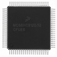
MCHC912B32CFUE8 Freescale Semiconductor, MCHC912B32CFUE8 Datasheet - Page 265

MCHC912B32CFUE8
Manufacturer Part Number
MCHC912B32CFUE8
Description
IC MCU 32K FLASH 8MHZ 80-QFP
Manufacturer
Freescale Semiconductor
Series
HC12r
Datasheet
1.MCHC912B32CFUE8.pdf
(334 pages)
Specifications of MCHC912B32CFUE8
Core Processor
CPU12
Core Size
16-Bit
Speed
8MHz
Connectivity
SCI, SPI
Peripherals
POR, PWM, WDT
Number Of I /o
63
Program Memory Size
32KB (32K x 8)
Program Memory Type
FLASH
Eeprom Size
768 x 8
Ram Size
1K x 8
Voltage - Supply (vcc/vdd)
4.5 V ~ 5.5 V
Data Converters
A/D 8x10b
Oscillator Type
External
Operating Temperature
-40°C ~ 85°C
Package / Case
80-QFP
Cpu Family
HC12
Device Core Size
16b
Frequency (max)
8MHz
Interface Type
SCI/SPI
Total Internal Ram Size
1KB
# I/os (max)
63
Operating Supply Voltage (typ)
5V
Operating Supply Voltage (max)
5.5V
Operating Supply Voltage (min)
4.5V
On-chip Adc
8-chx10-bit
Instruction Set Architecture
CISC
Operating Temp Range
-40C to 85C
Operating Temperature Classification
Industrial
Mounting
Surface Mount
Pin Count
80
Package Type
PQFP
Package
80PQFP
Family Name
HC12
Maximum Speed
8 MHz
Operating Supply Voltage
5 V
Data Bus Width
16 Bit
Number Of Programmable I/os
63
Processor Series
HC912B
Core
HC12
Data Ram Size
1 KB
Maximum Clock Frequency
8 MHz
Maximum Operating Temperature
+ 85 C
Mounting Style
SMD/SMT
3rd Party Development Tools
EWHCS12
Development Tools By Supplier
M68EVB912B32E
Minimum Operating Temperature
- 40 C
Lead Free Status / RoHS Status
Lead free / RoHS Compliant
Available stocks
Company
Part Number
Manufacturer
Quantity
Price
Company:
Part Number:
MCHC912B32CFUE8
Manufacturer:
Freescale Semiconductor
Quantity:
10 000
- Current page: 265 of 334
- Download datasheet (2Mb)
16.12.4 msCAN12 Bus Timing Register 1
SAMP — Sampling Bit
TSEG22–TSEG10 — Time Segment Bits
1. In this case, PHASE_SEG1 must be at least two times quanta.
Freescale Semiconductor
This bit determines the number of samples of the serial bus to be taken per bit time. If set, three
samples per bit are taken, the regular one (sample point) and two preceding samples, using a majority
rule. For higher bit rates, SAMP should be cleared, which means that only one sample will be taken
per bit.
Time segments within the bit time fix the number of clock cycles per bit time and the location of the
sample point. See
Time segment 1 (TSEG1) and time segment 2 (TSEG2) are programmable as shown in
SYNC_SEG
Transmit point
Sample point
0 = One sample per bit
1 = Three samples per bit.
Address: $0103
Reset:
Read:
Write:
System expects transitions to occur on the bus during this period.
A node in transmit mode will transfer a new value to the CAN bus at this point.
A node in receive mode will sample the bus at this point. If the three samples per bit option is
selected, then this point marks the position of the third sample.
TSEG13
Figure
Figure 16-19. msCAN12 Bus Timing Register 1 (CBTR1)
SAMP
Bit 7
0
0
0
0
1
.
0
16-7.
TSEG22
(1)
TSEG12
TSEG22
6
0
Table 16-7. Time Segment Syntax
Table 16-8. Time Segment Values
M68HC12B Family Data Sheet, Rev. 9.1
0
0
0
0
1
0
0
1
.
.
TSEG21
5
0
TSEG11
TSEG21
0
0
1
1
1
0
0
1
.
.
TSEG20
4
0
TSEG10
TSEG20
TSEG13
0
1
0
1
1
0
1
1
.
.
3
0
Programmer’s Model of Control Registers
TSEG12
16 Tq clock cycles
Time Segment 1
Time Segment 2
2 Tq clock cycles
3 Tq clock cycles
4 Tq clock cycles
2 Tq clock cycles
8 Tq clock cycles
1 Tq clock cycle
1 Tq clock cycle
2
0
.
.
TSEG11
1
0
TSEG10
Bit 0
0
Table
16-8.
265
Related parts for MCHC912B32CFUE8
Image
Part Number
Description
Manufacturer
Datasheet
Request
R
Part Number:
Description:
Manufacturer:
Freescale Semiconductor, Inc
Datasheet:
Part Number:
Description:
Manufacturer:
Freescale Semiconductor, Inc
Datasheet:
Part Number:
Description:
Manufacturer:
Freescale Semiconductor, Inc
Datasheet:
Part Number:
Description:
Manufacturer:
Freescale Semiconductor, Inc
Datasheet:
Part Number:
Description:
Manufacturer:
Freescale Semiconductor, Inc
Datasheet:
Part Number:
Description:
Manufacturer:
Freescale Semiconductor, Inc
Datasheet:
Part Number:
Description:
Manufacturer:
Freescale Semiconductor, Inc
Datasheet:
Part Number:
Description:
Manufacturer:
Freescale Semiconductor, Inc
Datasheet:
Part Number:
Description:
Manufacturer:
Freescale Semiconductor, Inc
Datasheet:
Part Number:
Description:
Manufacturer:
Freescale Semiconductor, Inc
Datasheet:
Part Number:
Description:
Manufacturer:
Freescale Semiconductor, Inc
Datasheet:
Part Number:
Description:
Manufacturer:
Freescale Semiconductor, Inc
Datasheet:
Part Number:
Description:
Manufacturer:
Freescale Semiconductor, Inc
Datasheet:
Part Number:
Description:
Manufacturer:
Freescale Semiconductor, Inc
Datasheet:
Part Number:
Description:
Manufacturer:
Freescale Semiconductor, Inc
Datasheet:


