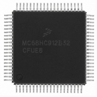
MCHC912B32CFUE8 Freescale Semiconductor, MCHC912B32CFUE8 Datasheet - Page 320

MCHC912B32CFUE8
Manufacturer Part Number
MCHC912B32CFUE8
Description
IC MCU 32K FLASH 8MHZ 80-QFP
Manufacturer
Freescale Semiconductor
Series
HC12r
Datasheet
1.MCHC912B32CFUE8.pdf
(334 pages)
Specifications of MCHC912B32CFUE8
Core Processor
CPU12
Core Size
16-Bit
Speed
8MHz
Connectivity
SCI, SPI
Peripherals
POR, PWM, WDT
Number Of I /o
63
Program Memory Size
32KB (32K x 8)
Program Memory Type
FLASH
Eeprom Size
768 x 8
Ram Size
1K x 8
Voltage - Supply (vcc/vdd)
4.5 V ~ 5.5 V
Data Converters
A/D 8x10b
Oscillator Type
External
Operating Temperature
-40°C ~ 85°C
Package / Case
80-QFP
Cpu Family
HC12
Device Core Size
16b
Frequency (max)
8MHz
Interface Type
SCI/SPI
Total Internal Ram Size
1KB
# I/os (max)
63
Operating Supply Voltage (typ)
5V
Operating Supply Voltage (max)
5.5V
Operating Supply Voltage (min)
4.5V
On-chip Adc
8-chx10-bit
Instruction Set Architecture
CISC
Operating Temp Range
-40C to 85C
Operating Temperature Classification
Industrial
Mounting
Surface Mount
Pin Count
80
Package Type
PQFP
Package
80PQFP
Family Name
HC12
Maximum Speed
8 MHz
Operating Supply Voltage
5 V
Data Bus Width
16 Bit
Number Of Programmable I/os
63
Processor Series
HC912B
Core
HC12
Data Ram Size
1 KB
Maximum Clock Frequency
8 MHz
Maximum Operating Temperature
+ 85 C
Mounting Style
SMD/SMT
3rd Party Development Tools
EWHCS12
Development Tools By Supplier
M68EVB912B32E
Minimum Operating Temperature
- 40 C
Lead Free Status / RoHS Status
Lead free / RoHS Compliant
Available stocks
Company
Part Number
Manufacturer
Quantity
Price
Company:
Part Number:
MCHC912B32CFUE8
Manufacturer:
Freescale Semiconductor
Quantity:
10 000
- Current page: 320 of 334
- Download datasheet (2Mb)
Electrical Specifications
19.14 Control Timing
320
Frequency of operation
E-clock period
Crystal frequency
External oscillator frequency
Processor control setup time
Reset input pulse width
Mode programming setup time
Mode programming hold time
Interrupt pulse width, IRQ edge-sensitive mode
Wait recovery startup time
Timer input capture pulse width
Pulse accumulator pulse width
1. RESET is recognized during the first clock cycle it is held low. Internal circuitry then drives the pin low for 16 clock cycles,
t
To guarantee external reset vector
Minimum input time (can be pre-empted by internal reset)
PW
t
PW
PCSU
WRS
releases the pin, and samples the pin level eight cycles later to determine the source of the interrupt.
IRQ
TIM
= 4 t
= t
= 2 t
= 2 t
cyc
cyc
Notes:
PT7
PT7
PT7–PT0
PT7–PT0
/2+ 20
cyc
cyc
1. Rising edge sensitive input
2. Falling edge sensitive input
1
2
+ 20
+ 20
(1)
(2)
(1)
Characteristic
PW
PW
TIM
PA
M68HC12B Family Data Sheet, Rev. 9.1
Figure 19-5. Timer Inputs
PW
Symbol
PW
PW
PW
t
f
t
t
PCSU
t
XTAL
2 f
WRS
t
MPS
MPH
cyc
f
RSTL
o
IRQ
TIM
o
PA
TBD
Min
125
270
270
82
32
10
dc
—
dc
—
2
4
8.0 MHz
Freescale Semiconductor
Max
16.0
16.0
8.0
—
—
—
—
—
—
—
—
—
4
MHz
MHz
MHz
Unit
t
t
t
ns
ns
ns
ns
ns
ns
cyc
cyc
cyc
Related parts for MCHC912B32CFUE8
Image
Part Number
Description
Manufacturer
Datasheet
Request
R
Part Number:
Description:
Manufacturer:
Freescale Semiconductor, Inc
Datasheet:
Part Number:
Description:
Manufacturer:
Freescale Semiconductor, Inc
Datasheet:
Part Number:
Description:
Manufacturer:
Freescale Semiconductor, Inc
Datasheet:
Part Number:
Description:
Manufacturer:
Freescale Semiconductor, Inc
Datasheet:
Part Number:
Description:
Manufacturer:
Freescale Semiconductor, Inc
Datasheet:
Part Number:
Description:
Manufacturer:
Freescale Semiconductor, Inc
Datasheet:
Part Number:
Description:
Manufacturer:
Freescale Semiconductor, Inc
Datasheet:
Part Number:
Description:
Manufacturer:
Freescale Semiconductor, Inc
Datasheet:
Part Number:
Description:
Manufacturer:
Freescale Semiconductor, Inc
Datasheet:
Part Number:
Description:
Manufacturer:
Freescale Semiconductor, Inc
Datasheet:
Part Number:
Description:
Manufacturer:
Freescale Semiconductor, Inc
Datasheet:
Part Number:
Description:
Manufacturer:
Freescale Semiconductor, Inc
Datasheet:
Part Number:
Description:
Manufacturer:
Freescale Semiconductor, Inc
Datasheet:
Part Number:
Description:
Manufacturer:
Freescale Semiconductor, Inc
Datasheet:
Part Number:
Description:
Manufacturer:
Freescale Semiconductor, Inc
Datasheet:


