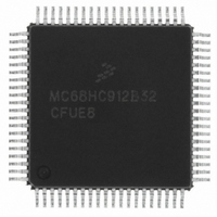
MCHC912B32CFUE8 Freescale Semiconductor, MCHC912B32CFUE8 Datasheet - Page 120

MCHC912B32CFUE8
Manufacturer Part Number
MCHC912B32CFUE8
Description
IC MCU 32K FLASH 8MHZ 80-QFP
Manufacturer
Freescale Semiconductor
Series
HC12r
Datasheet
1.MCHC912B32CFUE8.pdf
(334 pages)
Specifications of MCHC912B32CFUE8
Core Processor
CPU12
Core Size
16-Bit
Speed
8MHz
Connectivity
SCI, SPI
Peripherals
POR, PWM, WDT
Number Of I /o
63
Program Memory Size
32KB (32K x 8)
Program Memory Type
FLASH
Eeprom Size
768 x 8
Ram Size
1K x 8
Voltage - Supply (vcc/vdd)
4.5 V ~ 5.5 V
Data Converters
A/D 8x10b
Oscillator Type
External
Operating Temperature
-40°C ~ 85°C
Package / Case
80-QFP
Cpu Family
HC12
Device Core Size
16b
Frequency (max)
8MHz
Interface Type
SCI/SPI
Total Internal Ram Size
1KB
# I/os (max)
63
Operating Supply Voltage (typ)
5V
Operating Supply Voltage (max)
5.5V
Operating Supply Voltage (min)
4.5V
On-chip Adc
8-chx10-bit
Instruction Set Architecture
CISC
Operating Temp Range
-40C to 85C
Operating Temperature Classification
Industrial
Mounting
Surface Mount
Pin Count
80
Package Type
PQFP
Package
80PQFP
Family Name
HC12
Maximum Speed
8 MHz
Operating Supply Voltage
5 V
Data Bus Width
16 Bit
Number Of Programmable I/os
63
Processor Series
HC912B
Core
HC12
Data Ram Size
1 KB
Maximum Clock Frequency
8 MHz
Maximum Operating Temperature
+ 85 C
Mounting Style
SMD/SMT
3rd Party Development Tools
EWHCS12
Development Tools By Supplier
M68EVB912B32E
Minimum Operating Temperature
- 40 C
Lead Free Status / RoHS Status
Lead free / RoHS Compliant
Available stocks
Company
Part Number
Manufacturer
Quantity
Price
Company:
Part Number:
MCHC912B32CFUE8
Manufacturer:
Freescale Semiconductor
Quantity:
10 000
- Current page: 120 of 334
- Download datasheet (2Mb)
Clock Generation Module (CGM)
FCOP — Force COP Watchdog Reset Bit
DISR — Disable Resets from COP Watchdog and Clock Monitor Bit
CR2, CR1, and CR0 — COP Watchdog Timer Rate Select Bit
10.7.5 Arm/Reset COP Timer Register
Always reads $00.
Writing $55 to this address is the first step of the COP watchdog sequence.
Writing $AA to this address is the second step of the COP watchdog sequence. Other instructions may
be executed between these writes but both must be completed in the correct order prior to timeout to
avoid a watchdog reset. Writing anything other than $55 or $AA causes a COP reset to occur.
120
Writes are not allowed in normal modes; can be written anytime in special modes.
If DISR is set, this bit has no effect.
Writes are not allowed in normal modes, anytime in special modes.
The COP system is driven by a constant frequency of E/2
but two stages of this divider to be bypassed for testing in special modes only.) These bits specify an
additional division factor to arrive at the COP timeout rate. The clock used for this module is the E
clock.
Write once in normal modes, anytime in special modes.
0 = Normal operation
1 = Force a COP reset, if COP is enabled.
0 = Normal operation
1 = Regardless of other control bit states, COP and clock monitor do not generate a system reset.
CR2
Address: $0017
0
0
0
0
1
1
1
1
Reset:
Read:
Write:
CR1
0
0
1
1
0
0
1
1
Figure 10-9. Arm/Reset COP Timer Register (COPRST)
Bit 7
Bit 7
0
Table 10-4. COP Watchdog Rates (RTBYP = 0)
CR0
0
1
0
1
0
1
0
1
Bit 6
6
0
M68HC12B Family Data Sheet, Rev. 9.1
Divide E By:
OFF
2
2
2
2
2
2
2
Bit 5
13
15
17
19
21
22
23
5
0
Bit 4
4
0
At E = 4.0-MHz
0 to +2.048 ms
131.072 ms
524.288 ms
8.1920 ms
32.768 ms
2.048 ms
Timeout
1.048 s
2.097 s
OFF
Bit 3
13
3
0
. (RTBYP in the RTICTL register allows all
Bit 2
2
0
At E = 8.0-MHz
0 to +1.024 ms
262.144 ms
524.288 ms
1.048576 s
Bit 1
16.384 ms
65.536 ms
1.024 ms
4.096 ms
Timeout
1
0
OFF
Freescale Semiconductor
Bit 0
Bit 0
0
Related parts for MCHC912B32CFUE8
Image
Part Number
Description
Manufacturer
Datasheet
Request
R
Part Number:
Description:
Manufacturer:
Freescale Semiconductor, Inc
Datasheet:
Part Number:
Description:
Manufacturer:
Freescale Semiconductor, Inc
Datasheet:
Part Number:
Description:
Manufacturer:
Freescale Semiconductor, Inc
Datasheet:
Part Number:
Description:
Manufacturer:
Freescale Semiconductor, Inc
Datasheet:
Part Number:
Description:
Manufacturer:
Freescale Semiconductor, Inc
Datasheet:
Part Number:
Description:
Manufacturer:
Freescale Semiconductor, Inc
Datasheet:
Part Number:
Description:
Manufacturer:
Freescale Semiconductor, Inc
Datasheet:
Part Number:
Description:
Manufacturer:
Freescale Semiconductor, Inc
Datasheet:
Part Number:
Description:
Manufacturer:
Freescale Semiconductor, Inc
Datasheet:
Part Number:
Description:
Manufacturer:
Freescale Semiconductor, Inc
Datasheet:
Part Number:
Description:
Manufacturer:
Freescale Semiconductor, Inc
Datasheet:
Part Number:
Description:
Manufacturer:
Freescale Semiconductor, Inc
Datasheet:
Part Number:
Description:
Manufacturer:
Freescale Semiconductor, Inc
Datasheet:
Part Number:
Description:
Manufacturer:
Freescale Semiconductor, Inc
Datasheet:
Part Number:
Description:
Manufacturer:
Freescale Semiconductor, Inc
Datasheet:


