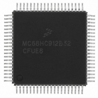
MCHC912B32CFUE8 Freescale Semiconductor, MCHC912B32CFUE8 Datasheet - Page 202

MCHC912B32CFUE8
Manufacturer Part Number
MCHC912B32CFUE8
Description
IC MCU 32K FLASH 8MHZ 80-QFP
Manufacturer
Freescale Semiconductor
Series
HC12r
Datasheet
1.MCHC912B32CFUE8.pdf
(334 pages)
Specifications of MCHC912B32CFUE8
Core Processor
CPU12
Core Size
16-Bit
Speed
8MHz
Connectivity
SCI, SPI
Peripherals
POR, PWM, WDT
Number Of I /o
63
Program Memory Size
32KB (32K x 8)
Program Memory Type
FLASH
Eeprom Size
768 x 8
Ram Size
1K x 8
Voltage - Supply (vcc/vdd)
4.5 V ~ 5.5 V
Data Converters
A/D 8x10b
Oscillator Type
External
Operating Temperature
-40°C ~ 85°C
Package / Case
80-QFP
Cpu Family
HC12
Device Core Size
16b
Frequency (max)
8MHz
Interface Type
SCI/SPI
Total Internal Ram Size
1KB
# I/os (max)
63
Operating Supply Voltage (typ)
5V
Operating Supply Voltage (max)
5.5V
Operating Supply Voltage (min)
4.5V
On-chip Adc
8-chx10-bit
Instruction Set Architecture
CISC
Operating Temp Range
-40C to 85C
Operating Temperature Classification
Industrial
Mounting
Surface Mount
Pin Count
80
Package Type
PQFP
Package
80PQFP
Family Name
HC12
Maximum Speed
8 MHz
Operating Supply Voltage
5 V
Data Bus Width
16 Bit
Number Of Programmable I/os
63
Processor Series
HC912B
Core
HC12
Data Ram Size
1 KB
Maximum Clock Frequency
8 MHz
Maximum Operating Temperature
+ 85 C
Mounting Style
SMD/SMT
3rd Party Development Tools
EWHCS12
Development Tools By Supplier
M68EVB912B32E
Minimum Operating Temperature
- 40 C
Lead Free Status / RoHS Status
Lead free / RoHS Compliant
Available stocks
Company
Part Number
Manufacturer
Quantity
Price
Company:
Part Number:
MCHC912B32CFUE8
Manufacturer:
Freescale Semiconductor
Quantity:
10 000
- Current page: 202 of 334
- Download datasheet (2Mb)
Serial Interface
14.3.1 SPI Baud Rate Generation
The P clock is input to a divider series and the resulting SPI clock rate may be selected to be P divided
by 2, 4, 8, 16, 32, 64, 128, or 256. Three bits in the SP0BR register control the SPI clock rate. This baud
rate generator is activated only when SPI is in the master mode and serial transfer is taking place.
Otherwise, this divider is disabled to save power.
14.3.2 SPI Operation
In the SPI system, the 8-bit data register in the master and the 8-bit data register in the slave are linked
to form a distributed 16-bit register. When a data transfer operation is performed, this 16-bit register is
serially shifted eight bit positions by the SCK clock from the master so the data is effectively exchanged
between the master and the slave. Data written to the SP0DR register of the master becomes the output
data for the slave and data read from the SP0DR register of the master after a transfer operation is the
input data from the slave.
A clock phase control bit (CPHA) and a clock polarity control bit (CPOL) in the SPI control register 1
(SP0CR1) select one of four possible clock formats to be used by the SPI system. The CPOL bit simply
selects non-inverted or inverted clock. The CPHA bit is used to accommodate two fundamentally different
protocols by shifting the clock by one half cycle or no phase shift.
202
SCK (CPOL = 0)
SCK (CPOL = 1)
SAMPLE I
CHANGE O
MOSI PIN
CHANGE O
MISO PIN
SEL SS (O)
MASTER ONLY
SEL SS (I)
MOSI/MISO
MSB first (LSBF = 0) :
LSB first (LSBF = 1) :
TRANSFER
t
L
Figure 14-12. SPI Clock Format 0 (CPHA = 0)
MSB
LSB
M68HC12B Family Data Sheet, Rev. 9.1
BEGIN
Bit 6
Bit 1
Bit 5
Bit 2
Bit 4
Bit 3
Bit 3
Bit 4
Bit 2
Bit 5
Bit 1
Bit 6
END
MSB
LSB
Freescale Semiconductor
Minimum 1/2 SCK
t
T
for t
T
t
, t
I
l
, t
L
t
L
Related parts for MCHC912B32CFUE8
Image
Part Number
Description
Manufacturer
Datasheet
Request
R
Part Number:
Description:
Manufacturer:
Freescale Semiconductor, Inc
Datasheet:
Part Number:
Description:
Manufacturer:
Freescale Semiconductor, Inc
Datasheet:
Part Number:
Description:
Manufacturer:
Freescale Semiconductor, Inc
Datasheet:
Part Number:
Description:
Manufacturer:
Freescale Semiconductor, Inc
Datasheet:
Part Number:
Description:
Manufacturer:
Freescale Semiconductor, Inc
Datasheet:
Part Number:
Description:
Manufacturer:
Freescale Semiconductor, Inc
Datasheet:
Part Number:
Description:
Manufacturer:
Freescale Semiconductor, Inc
Datasheet:
Part Number:
Description:
Manufacturer:
Freescale Semiconductor, Inc
Datasheet:
Part Number:
Description:
Manufacturer:
Freescale Semiconductor, Inc
Datasheet:
Part Number:
Description:
Manufacturer:
Freescale Semiconductor, Inc
Datasheet:
Part Number:
Description:
Manufacturer:
Freescale Semiconductor, Inc
Datasheet:
Part Number:
Description:
Manufacturer:
Freescale Semiconductor, Inc
Datasheet:
Part Number:
Description:
Manufacturer:
Freescale Semiconductor, Inc
Datasheet:
Part Number:
Description:
Manufacturer:
Freescale Semiconductor, Inc
Datasheet:
Part Number:
Description:
Manufacturer:
Freescale Semiconductor, Inc
Datasheet:


