HD64F7144F50V Renesas Electronics America, HD64F7144F50V Datasheet - Page 196
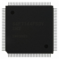
HD64F7144F50V
Manufacturer Part Number
HD64F7144F50V
Description
IC SUPERH MCU FLASH 256K 112QFP
Manufacturer
Renesas Electronics America
Series
SuperH® SH7144r
Specifications of HD64F7144F50V
Core Processor
SH-2
Core Size
32-Bit
Speed
50MHz
Connectivity
EBI/EMI, I²C, SCI
Peripherals
DMA, POR, PWM, WDT
Number Of I /o
74
Program Memory Size
256KB (256K x 8)
Program Memory Type
FLASH
Ram Size
8K x 8
Voltage - Supply (vcc/vdd)
3 V ~ 3.6 V
Data Converters
A/D 8x10b
Oscillator Type
Internal
Operating Temperature
-20°C ~ 75°C
Package / Case
112-QFP
For Use With
HS0005KCU11H - EMULATOR E10A-USB H8S(X),SH2(A)EDK7145 - DEV EVALUATION KIT SH7145
Lead Free Status / RoHS Status
Lead free / RoHS Compliant
Eeprom Size
-
Available stocks
Company
Part Number
Manufacturer
Quantity
Price
Company:

Part Number:
HD64F7144F50V
Manufacturer:
RENESAS
Quantity:
450
Company:
Part Number:
HD64F7144F50V
Manufacturer:
Renesas Electronics America
Quantity:
10 000
Part Number:
HD64F7144F50V
Manufacturer:
RENESAS/瑞萨
Quantity:
20 000


Section 6 Instruction Descriptions
6.1.28
Format
LDRE @(disp,PC) disp
Description: Stores the effective address of the source operand in the repeat end register RE. The
effective address is an address specified by PC + displacement. The PC is the address four bytes
after this instruction. The 8-bit displacement is sign-extended and doubled. Consequently, the
relative interval from the branch destination is –256 to +254 bytes.
Note: The effective address value designated for the RE reregister is different from the actual
Operation:
Rev. 5.00 Jun 30, 2004 page 180 of 512
REJ09B0171-0500O
LDRE(long d) /* LDRE @(disp, PC) */
{
}
long disp;
if ((d&0x80)==0) disp=(0x000000FF & (long)d);
else disp=(0xFFFFFF00 | (long)d);
RE=PC+(disp<<1);
PC+=2;
repeat end address. Refer to table 4.35, RS and RE Design Rule, for more information.
When this instruction is arranged immediately after the delayed branch instruction, PC
becomes the "first address +2" of the branch destination.
LDRE (Load Effective Address to RE Register): System Control Instruction
Abstract
RE
2 + PC
Code
10001110dddddddd 1
Cycle T Bit SH-1 SH-2
—
—
Instructions
Applicable
—
SH-
DSP
Related parts for HD64F7144F50V
Image
Part Number
Description
Manufacturer
Datasheet
Request
R


Part Number:
Description:
KIT STARTER FOR M16C/29
Manufacturer:
Renesas Electronics America
Datasheet:

Part Number:
Description:
KIT STARTER FOR R8C/2D
Manufacturer:
Renesas Electronics America
Datasheet:

Part Number:
Description:
R0K33062P STARTER KIT
Manufacturer:
Renesas Electronics America
Datasheet:

Part Number:
Description:
KIT STARTER FOR R8C/23 E8A
Manufacturer:
Renesas Electronics America
Datasheet:

Part Number:
Description:
KIT STARTER FOR R8C/25
Manufacturer:
Renesas Electronics America
Datasheet:

Part Number:
Description:
KIT STARTER H8S2456 SHARPE DSPLY
Manufacturer:
Renesas Electronics America
Datasheet:

Part Number:
Description:
KIT STARTER FOR R8C38C
Manufacturer:
Renesas Electronics America
Datasheet:

Part Number:
Description:
KIT STARTER FOR R8C35C
Manufacturer:
Renesas Electronics America
Datasheet:

Part Number:
Description:
KIT STARTER FOR R8CL3AC+LCD APPS
Manufacturer:
Renesas Electronics America
Datasheet:
Part Number:
Description:
KIT STARTER FOR RX610
Manufacturer:
Renesas Electronics America
Datasheet:

Part Number:
Description:
KIT STARTER FOR R32C/118
Manufacturer:
Renesas Electronics America
Datasheet:

Part Number:
Description:
KIT DEV RSK-R8C/26-29
Manufacturer:
Renesas Electronics America
Datasheet:

Part Number:
Description:
KIT STARTER FOR SH7124
Manufacturer:
Renesas Electronics America
Datasheet:

Part Number:
Description:
KIT STARTER FOR H8SX/1622
Manufacturer:
Renesas Electronics America
Datasheet: