HD64F7144F50V Renesas Electronics America, HD64F7144F50V Datasheet - Page 239
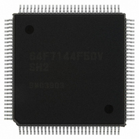
HD64F7144F50V
Manufacturer Part Number
HD64F7144F50V
Description
IC SUPERH MCU FLASH 256K 112QFP
Manufacturer
Renesas Electronics America
Series
SuperH® SH7144r
Specifications of HD64F7144F50V
Core Processor
SH-2
Core Size
32-Bit
Speed
50MHz
Connectivity
EBI/EMI, I²C, SCI
Peripherals
DMA, POR, PWM, WDT
Number Of I /o
74
Program Memory Size
256KB (256K x 8)
Program Memory Type
FLASH
Ram Size
8K x 8
Voltage - Supply (vcc/vdd)
3 V ~ 3.6 V
Data Converters
A/D 8x10b
Oscillator Type
Internal
Operating Temperature
-20°C ~ 75°C
Package / Case
112-QFP
For Use With
HS0005KCU11H - EMULATOR E10A-USB H8S(X),SH2(A)EDK7145 - DEV EVALUATION KIT SH7145
Lead Free Status / RoHS Status
Lead free / RoHS Compliant
Eeprom Size
-
Available stocks
Company
Part Number
Manufacturer
Quantity
Price
Company:

Part Number:
HD64F7144F50V
Manufacturer:
RENESAS
Quantity:
450
Company:
Part Number:
HD64F7144F50V
Manufacturer:
Renesas Electronics America
Quantity:
10 000
Part Number:
HD64F7144F50V
Manufacturer:
RENESAS/瑞萨
Quantity:
20 000


6.1.46
Description: Logically ORs the contents of general registers Rn and Rm, and stores the result in
Rn. The contents of general register R0 can also be ORed with zero-extended 8-bit immediate
data, or 8-bit memory data accessed by using indirect indexed GBR addressing can be ORed with
8-bit immediate data.
Operation:
Format
OR
OR
OR.B #imm,@(R0,GBR)
OR(long m,long n)
{
}
ORI(long i)
{
}
ORM(long i)
{
}
Rm,Rn
#imm,R0
R[n]|=R[m];
PC+=2;
R[0]|=(0x000000FF & (long)i);
PC+=2;
long temp;
temp=(long)Read_Byte(GBR+R[0]);
temp|=(0x000000FF & (long)i);
Write_Byte(GBR+R[0],temp);
PC+=2;
OR (OR Logical) Logic Operation Instruction
/* OR #imm,R0 */
/* OR.B #imm,@(R0,GBR) */
Abstract
Rn | Rm
R0 | imm
(R0 + GBR) |
imm
/* OR Rm,Rn */
(R0 + GBR)
Rn
R0
Code
0010nnnnmmmm1011
11001011iiiiiiii
11001111iiiiiiii
Rev. 5.00 Jun 30, 2004 page 223 of 512
Section 6 Instruction Descriptions
Cycle
1
1
3
T
Bit SH-1
—
—
—
REJ09B0171-0500O
Instructions
Applicable
SH-2
SH-
DSP
Related parts for HD64F7144F50V
Image
Part Number
Description
Manufacturer
Datasheet
Request
R


Part Number:
Description:
KIT STARTER FOR M16C/29
Manufacturer:
Renesas Electronics America
Datasheet:

Part Number:
Description:
KIT STARTER FOR R8C/2D
Manufacturer:
Renesas Electronics America
Datasheet:

Part Number:
Description:
R0K33062P STARTER KIT
Manufacturer:
Renesas Electronics America
Datasheet:

Part Number:
Description:
KIT STARTER FOR R8C/23 E8A
Manufacturer:
Renesas Electronics America
Datasheet:

Part Number:
Description:
KIT STARTER FOR R8C/25
Manufacturer:
Renesas Electronics America
Datasheet:

Part Number:
Description:
KIT STARTER H8S2456 SHARPE DSPLY
Manufacturer:
Renesas Electronics America
Datasheet:

Part Number:
Description:
KIT STARTER FOR R8C38C
Manufacturer:
Renesas Electronics America
Datasheet:

Part Number:
Description:
KIT STARTER FOR R8C35C
Manufacturer:
Renesas Electronics America
Datasheet:

Part Number:
Description:
KIT STARTER FOR R8CL3AC+LCD APPS
Manufacturer:
Renesas Electronics America
Datasheet:
Part Number:
Description:
KIT STARTER FOR RX610
Manufacturer:
Renesas Electronics America
Datasheet:

Part Number:
Description:
KIT STARTER FOR R32C/118
Manufacturer:
Renesas Electronics America
Datasheet:

Part Number:
Description:
KIT DEV RSK-R8C/26-29
Manufacturer:
Renesas Electronics America
Datasheet:

Part Number:
Description:
KIT STARTER FOR SH7124
Manufacturer:
Renesas Electronics America
Datasheet:

Part Number:
Description:
KIT STARTER FOR H8SX/1622
Manufacturer:
Renesas Electronics America
Datasheet: