HD64F7144F50V Renesas Electronics America, HD64F7144F50V Datasheet - Page 294
HD64F7144F50V
Manufacturer Part Number
HD64F7144F50V
Description
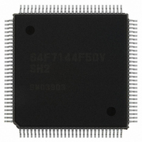
IC SUPERH MCU FLASH 256K 112QFP
Manufacturer
Renesas Electronics America
Series
SuperH® SH7144r
Specifications of HD64F7144F50V
Core Processor
SH-2
Core Size
32-Bit
Speed
50MHz
Connectivity
EBI/EMI, I²C, SCI
Peripherals
DMA, POR, PWM, WDT
Number Of I /o
74
Program Memory Size
256KB (256K x 8)
Program Memory Type
FLASH
Ram Size
8K x 8
Voltage - Supply (vcc/vdd)
3 V ~ 3.6 V
Data Converters
A/D 8x10b
Oscillator Type
Internal
Operating Temperature
-20°C ~ 75°C
Package / Case
112-QFP
For Use With
HS0005KCU11H - EMULATOR E10A-USB H8S(X),SH2(A)EDK7145 - DEV EVALUATION KIT SH7145
Lead Free Status / RoHS Status
Lead free / RoHS Compliant
Eeprom Size
-
Available stocks
Company
Part Number
Manufacturer
Quantity
Price
Company:

Part Number:
HD64F7144F50V
Manufacturer:
RENESAS
Quantity:
450
Company:
Part Number:
HD64F7144F50V
Manufacturer:
Renesas Electronics America
Quantity:
10 000
Part Number:
HD64F7144F50V
Manufacturer:
RENESAS/瑞萨
Quantity:
20 000


Section 6 Instruction Descriptions
source operand is a register and the destination operand is memory, the top word of the register is
stored as the word data . In a longword transfer, the longword data is transferred. When the
destination operand is a register with guard bits, the sign is extended and stored in the guard bits.
Note: When one of the guard bit registers A0G and A1G is the source operand for store
Operation: See figure 6.17.
Rev. 5.00 Jun 30, 2004 page 278 of 512
REJ09B0171-0500O
processing, the data is output to the bottom 8 bits (bits 0–7) and the top 24 bits (bits 31–8)
become undefined.
Word data transfer
Sign extension
Longword data transfer
Sign extension
IDB: Main bus
31
31
S
S
31
31
Memory to register
Any memory area
Memory to register
Any memory area
Ds
16
As
Ds
As
Figure 6.17 The MOVS Instruction
15
Cleared
All 0
0
0
0
0
Post update
Post update
IDB[15:0]
IDB[31:0]
–2, 0,
+2, +lx
–4, 0,
+4, +lx
31
31
31
31
Register to memory
Register to memory
Any memory area
Any memory area
Ds
16
As
Ds
As
15
Ignored
0
0
0
0
Post update
Post update
–2, 0,
+2, +lx
–4, 0,
+4, +lx
Related parts for HD64F7144F50V
Image
Part Number
Description
Manufacturer
Datasheet
Request
R


Part Number:
Description:
KIT STARTER FOR M16C/29
Manufacturer:
Renesas Electronics America
Datasheet:

Part Number:
Description:
KIT STARTER FOR R8C/2D
Manufacturer:
Renesas Electronics America
Datasheet:

Part Number:
Description:
R0K33062P STARTER KIT
Manufacturer:
Renesas Electronics America
Datasheet:

Part Number:
Description:
KIT STARTER FOR R8C/23 E8A
Manufacturer:
Renesas Electronics America
Datasheet:

Part Number:
Description:
KIT STARTER FOR R8C/25
Manufacturer:
Renesas Electronics America
Datasheet:

Part Number:
Description:
KIT STARTER H8S2456 SHARPE DSPLY
Manufacturer:
Renesas Electronics America
Datasheet:

Part Number:
Description:
KIT STARTER FOR R8C38C
Manufacturer:
Renesas Electronics America
Datasheet:

Part Number:
Description:
KIT STARTER FOR R8C35C
Manufacturer:
Renesas Electronics America
Datasheet:

Part Number:
Description:
KIT STARTER FOR R8CL3AC+LCD APPS
Manufacturer:
Renesas Electronics America
Datasheet:
Part Number:
Description:
KIT STARTER FOR RX610
Manufacturer:
Renesas Electronics America
Datasheet:

Part Number:
Description:
KIT STARTER FOR R32C/118
Manufacturer:
Renesas Electronics America
Datasheet:

Part Number:
Description:
KIT DEV RSK-R8C/26-29
Manufacturer:
Renesas Electronics America
Datasheet:

Part Number:
Description:
KIT STARTER FOR SH7124
Manufacturer:
Renesas Electronics America
Datasheet:

Part Number:
Description:
KIT STARTER FOR H8SX/1622
Manufacturer:
Renesas Electronics America
Datasheet: