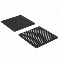
LPC3230FET296,551 NXP Semiconductors, LPC3230FET296,551 Datasheet - Page 2

LPC3230FET296,551
Manufacturer Part Number
LPC3230FET296,551
Description
IC ARM9 MCU 256K 296-TFBGA
Manufacturer
NXP Semiconductors
Series
LPC32x0r
Datasheet
1.OM11079.pdf
(77 pages)
Specifications of LPC3230FET296,551
Core Processor
ARM9
Core Size
16/32-Bit
Speed
266MHz
Connectivity
EBI/EMI, I²C, IrDA, Microwire, SPI, SSI, SSP, UART/USART, USB OTG
Peripherals
DMA, I²S, LCD, Motor Control PWM, PWM, WDT
Number Of I /o
51
Program Memory Type
ROMless
Ram Size
256K x 8
Voltage - Supply (vcc/vdd)
0.9 V ~ 3.6 V
Data Converters
A/D 3x10b
Oscillator Type
Internal
Operating Temperature
-40°C ~ 85°C
Package / Case
296-TFBGA
Processor Series
LPC32
Core
ARM926EJ-S
Data Bus Width
32 bit
Data Ram Size
256 KB
Interface Type
I2C, I2S, UART, USB
Maximum Clock Frequency
20 MHz
Number Of Programmable I/os
51
Number Of Timers
6
Operating Supply Voltage
2.7 V to 3.6 V
Maximum Operating Temperature
+ 85 C
Mounting Style
SMD/SMT
3rd Party Development Tools
MDK-ARM, RL-ARM, ULINK2
Minimum Operating Temperature
- 40 C
On-chip Adc
10 bit, 8 Channel
Lead Free Status / RoHS Status
Lead free / RoHS Compliant
Eeprom Size
-
Program Memory Size
-
Lead Free Status / Rohs Status
Details
Other names
568-4531
935287119551
935287119551
Available stocks
Company
Part Number
Manufacturer
Quantity
Price
Company:
Part Number:
LPC3230FET296,551
Manufacturer:
NXP Semiconductors
Quantity:
10 000
NXP Semiconductors
LPC3220_30_40_50_1
Product data sheet
Multi-layer AHB system that provides a separate bus for each AHB master, including
both an instruction and data bus for the CPU, two data busses for the DMA controller,
and another bus for the USB controller, one for the LCD, and a final one for the
Ethernet MAC. There are no arbitration delays in the system unless two masters
attempt to access the same slave at the same time.
External memory controller for DDR and SDR SDRAM as well as for static devices.
Two NAND flash controllers: One for single-level NAND flash devices and the other for
multi-level NAND flash devices.
Master Interrupt Controller (MIC) and two Slave Interrupt Controllers (SIC), supporting
74 interrupt sources.
Eight channel General Purpose DMA (GPDMA) controller on the AHB that can be
used with the SD card port, the high-speed UARTs, I
interfaces, as well as memory-to-memory transfers.
Serial interfaces:
Additional peripherals:
10/100 Ethernet MAC with dedicated DMA Controller.
USB interface supporting either device, host (OHCI compliant), or On-The-Go
(OTG) with an integral DMA controller and dedicated PLL to generate the required
48 MHz USB clock.
Four standard UARTs with fractional baud rate generation and 64 byte FIFOs. One
of the standard UARTs supports IrDA.
Three additional high-speed UARTs intended for on-board communications that
support baud rates up to 921 600 when using a 13 MHz main oscillator. All
high-speed UARTs provide 64 byte FIFOs.
Two SPI controllers.
Two SSP controllers.
Two I
support single master, slave, and multi-master I
Two I
channel can be operated independently on three pins, or both input and output
channels can be used with only four pins and a shared clock.
LCD controller supporting both STN and TFT panels, with dedicated DMA
controller. Programmable display resolution up to 1024 × 768.
Secure Digital (SD) memory card interface, which conforms to the SD Memory
Card Specification Version 1.01.
General Purpose (GP) input, output, and I/O pins. Includes 12 GP input pins, 24
GP output pins, and 51 GP I/O pins.
10-bit, 400 kHz Analog-to-Digital Converter (ADC) with input multiplexing from
three pins. Optionally, the ADC can operate as a touch screen controller.
Real-Time Clock (RTC) with separate power pin and dedicated 32 kHz oscillator.
NXP implemented the RTC in an independent on-chip power domain so it can
remain active while the rest of the chip is not powered. The RTC also includes a
32-byte scratch pad memory.
32-bit general purpose high-speed timer with a 16-bit pre-scaler. This timer
includes one external capture input pin and a capture connection to the RTC clock.
Interrupts may be generated using three match registers.
2
2
C-bus interfaces with standard open-drain pins. The I
S-bus interfaces, each with separate input and output channels. Each
All information provided in this document is subject to legal disclaimers.
Rev. 01.03 — 16 March 2010
LPC3220/30/40/50
2
C-bus configurations.
2
16/32-bit ARM microcontrollers
S-bus interfaces, and SPI
2
C-bus interfaces
© NXP B.V. 2010. All rights reserved.
2 of 77


