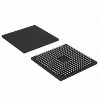
LPC3230FET296,551 NXP Semiconductors, LPC3230FET296,551 Datasheet - Page 59

LPC3230FET296,551
Manufacturer Part Number
LPC3230FET296,551
Description
IC ARM9 MCU 256K 296-TFBGA
Manufacturer
NXP Semiconductors
Series
LPC32x0r
Datasheet
1.OM11079.pdf
(77 pages)
Specifications of LPC3230FET296,551
Core Processor
ARM9
Core Size
16/32-Bit
Speed
266MHz
Connectivity
EBI/EMI, I²C, IrDA, Microwire, SPI, SSI, SSP, UART/USART, USB OTG
Peripherals
DMA, I²S, LCD, Motor Control PWM, PWM, WDT
Number Of I /o
51
Program Memory Type
ROMless
Ram Size
256K x 8
Voltage - Supply (vcc/vdd)
0.9 V ~ 3.6 V
Data Converters
A/D 3x10b
Oscillator Type
Internal
Operating Temperature
-40°C ~ 85°C
Package / Case
296-TFBGA
Processor Series
LPC32
Core
ARM926EJ-S
Data Bus Width
32 bit
Data Ram Size
256 KB
Interface Type
I2C, I2S, UART, USB
Maximum Clock Frequency
20 MHz
Number Of Programmable I/os
51
Number Of Timers
6
Operating Supply Voltage
2.7 V to 3.6 V
Maximum Operating Temperature
+ 85 C
Mounting Style
SMD/SMT
3rd Party Development Tools
MDK-ARM, RL-ARM, ULINK2
Minimum Operating Temperature
- 40 C
On-chip Adc
10 bit, 8 Channel
Lead Free Status / RoHS Status
Lead free / RoHS Compliant
Eeprom Size
-
Program Memory Size
-
Lead Free Status / Rohs Status
Details
Other names
568-4531
935287119551
935287119551
Available stocks
Company
Part Number
Manufacturer
Quantity
Price
Company:
Part Number:
LPC3230FET296,551
Manufacturer:
NXP Semiconductors
Quantity:
10 000
NXP Semiconductors
Table 14.
C
[1]
[2]
[3]
[4]
[5]
LPC3220_30_40_50_1
Product data sheet
Symbol Parameter
f
t
t
t
t
t
t
t
t
t
t
t
t
t
t
t
t
t
oper
CK
CL
CH
d(V)ctrl
h(ctrl)
d(AV)
h(A)
su(Q)
h(Q)
DQSH
DQSL
DQSS
DSS
DSH
d(DQS)
su(D)
h(D)
L
= 25 pF, T
All values valid for EMC pads set to fast slew rate at 1.8 V unless otherwise specified (see SDRAMCLK_CTRL register in the LPC32x0
User manual).
CMD_DLY = COMMAND_DELAY bitfield in SDRAMCLK_CTRL[18:14] register, see External memory controller (EMC) chapter in
LPC32x0 User manual.
Applies to signals EMC_DQM[1:0], EMC_DYCSm, EMC_RAS, EMC_CAS, EMC_WR, EMC_CKEm.
DQS_DELAY, see LPC32x0 user manual, External Memory Controller Chapter, Section 8 DDR DQS delay calibration for details on
configuring this value.
Test conditions for measurements: T
EMC_D[31:0] driving 2 inches of 50
resistors used. EMC pads set to fast slew rate at 1.8 V or 2.5 V (see SDRAMCLK_CTRL register in the LPC32x0 User manual).
operating frequency
clock cycle time
CK LOW-level width
CK HIGH-level width
control valid delay time
control hold time
address valid delay time
address hold time
data output set-up time
data output hold time
DQS HIGH time
DQS LOW time
WRITE command to first DQS latching
transition time
DQS falling edge to CK set-up time
DQS falling edge hold time from CK
DQS delay time
data input set-up time
data input hold time
EMC DDR SDRAM memory interface dynamic characteristics
amb
11.4 DDR SDRAM controller
= 25
°
C, unless otherwise specified.
Ω
amb
characteristic impedance trace with 10 pf capacitive load; no external source series termination
= −40 °C to +85 °C; operating frequency range f
All information provided in this document is subject to legal disclaimers.
Rev. 01.03 — 16 March 2010
Conditions
EMC_D and
EMC_DQM to
EMC_DQS
out
EMC_D and
EMC_DQM to
EMC_DQS
out
for WRITE
command
for WRITE
command
for DQS out
for DQS in
for DQS in
for DQS in
[2][3]
[2][3]
[2]
[2]
[5]
[5]
[4]
Min
-
7.5
-
-
-
-
-
-
0.08 ×
t
0.25 ×
t
-
-
-
-
-
-
-
-
CK
CK
[1]
Typical
104
9.6
0.5 × t
0.5 × t
(CMD_DLY × 0.25) + 1.5
(CMD_DLY × 0.25) − 1.5
(CMD_DLY × 0.25) + 1.5
(CMD_DLY × 0.25) − 1.5
0.15 × t
0.35 × t
0.5 × t
0.5 × t
t
0.5 × t
0.5 × t
DQS_DELAY
0.3
0.5
CK
LPC3220/30/40/50
oper
+ 0.7
= 52 MHz to 133 MHz; EMC_DQMm and
16/32-bit ARM microcontrollers
CK
CK
CK
CK
CK
CK
CK
CK
© NXP B.V. 2010. All rights reserved.
Max
133
-
-
-
-
-
-
-
0.25
× t
0.42
× t
-
-
-
-
-
-
-
-
CK
CK
59 of 77
Unit
MHz
ns
ns
ns
ns
ns
ns
ns
ns
ns
ns
ns
ns
ns
ns
ns
ns
ns


