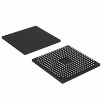
LPC3230FET296,551 NXP Semiconductors, LPC3230FET296,551 Datasheet - Page 51

LPC3230FET296,551
Manufacturer Part Number
LPC3230FET296,551
Description
IC ARM9 MCU 256K 296-TFBGA
Manufacturer
NXP Semiconductors
Series
LPC32x0r
Datasheet
1.OM11079.pdf
(77 pages)
Specifications of LPC3230FET296,551
Core Processor
ARM9
Core Size
16/32-Bit
Speed
266MHz
Connectivity
EBI/EMI, I²C, IrDA, Microwire, SPI, SSI, SSP, UART/USART, USB OTG
Peripherals
DMA, I²S, LCD, Motor Control PWM, PWM, WDT
Number Of I /o
51
Program Memory Type
ROMless
Ram Size
256K x 8
Voltage - Supply (vcc/vdd)
0.9 V ~ 3.6 V
Data Converters
A/D 3x10b
Oscillator Type
Internal
Operating Temperature
-40°C ~ 85°C
Package / Case
296-TFBGA
Processor Series
LPC32
Core
ARM926EJ-S
Data Bus Width
32 bit
Data Ram Size
256 KB
Interface Type
I2C, I2S, UART, USB
Maximum Clock Frequency
20 MHz
Number Of Programmable I/os
51
Number Of Timers
6
Operating Supply Voltage
2.7 V to 3.6 V
Maximum Operating Temperature
+ 85 C
Mounting Style
SMD/SMT
3rd Party Development Tools
MDK-ARM, RL-ARM, ULINK2
Minimum Operating Temperature
- 40 C
On-chip Adc
10 bit, 8 Channel
Lead Free Status / RoHS Status
Lead free / RoHS Compliant
Eeprom Size
-
Program Memory Size
-
Lead Free Status / Rohs Status
Details
Other names
568-4531
935287119551
935287119551
Available stocks
Company
Part Number
Manufacturer
Quantity
Price
Company:
Part Number:
LPC3230FET296,551
Manufacturer:
NXP Semiconductors
Quantity:
10 000
NXP Semiconductors
LPC3220_30_40_50_1
Product data sheet
10.1 Minimum core voltage requirements
10.2 Power supply sequencing
10.3 Power consumption per peripheral
Figure 4
frequency on pin VDD_CORE to ensure stable operation of the LPC3220/30/40/50.
The LPC32x0 has no power sequencing requirements, that is, V
and V
ensures that the system correctly powers up in the absence of core power. During IO
power-up this circuit takes care that the system is powered in a defined mode. The same
is valid for core power-down.
Table 9.
T
V
state at reset. Peripheral clocks are disabled except for peripheral measured.
[1]
Peripheral
High-speed UART (set to 115 200 Bd (8N1))
I
SSP
I
DMA
EMC
Multi-level NAND controller
Single-level NAND controller
LCD
Ethernet MAC
2
2
amb
Fig 4.
DD(IO)
C-bus
S
All three Ethernet clocks are in enabled in the MAC_CLK_CTRL register (see LPC32x0 User manual).
= 25
VDD_CORE
DDA(3V3)
= 1.8 V; USB AHB, IRAM, and IROM clocks always on; all peripherals are at their default
(V)
shows the minimum core supply voltage that should be applied for a given core
°
Minimum required core supply voltage for different core frequencies
1.4
1.2
1.0
0.8
C; CPU clock = 208 MHz; I-cache/D-cache, MMU disabled; VDD_CORE = 1.2 V;
Power consumption per peripheral
160
[1]
can be switched on or off independent of each other. An internal circuit
All information provided in this document is subject to legal disclaimers.
Rev. 01.03 — 16 March 2010
200
I
0.3
0.3
0.6
0.5
6.3
7.3
1.4
0.3
5.6
2.9
DD(run)
LPC3220/30/40/50
/ mA
240
16/32-bit ARM microcontrollers
core frequency (MHz)
DD(1V2)
, V
© NXP B.V. 2010. All rights reserved.
002aae872
DD(EMC)
280
, V
51 of 77
DD(IO)
,


