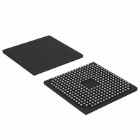
LPC3230FET296,551 NXP Semiconductors, LPC3230FET296,551 Datasheet - Page 38

LPC3230FET296,551
Manufacturer Part Number
LPC3230FET296,551
Description
IC ARM9 MCU 256K 296-TFBGA
Manufacturer
NXP Semiconductors
Series
LPC32x0r
Datasheet
1.OM11079.pdf
(77 pages)
Specifications of LPC3230FET296,551
Core Processor
ARM9
Core Size
16/32-Bit
Speed
266MHz
Connectivity
EBI/EMI, I²C, IrDA, Microwire, SPI, SSI, SSP, UART/USART, USB OTG
Peripherals
DMA, I²S, LCD, Motor Control PWM, PWM, WDT
Number Of I /o
51
Program Memory Type
ROMless
Ram Size
256K x 8
Voltage - Supply (vcc/vdd)
0.9 V ~ 3.6 V
Data Converters
A/D 3x10b
Oscillator Type
Internal
Operating Temperature
-40°C ~ 85°C
Package / Case
296-TFBGA
Processor Series
LPC32
Core
ARM926EJ-S
Data Bus Width
32 bit
Data Ram Size
256 KB
Interface Type
I2C, I2S, UART, USB
Maximum Clock Frequency
20 MHz
Number Of Programmable I/os
51
Number Of Timers
6
Operating Supply Voltage
2.7 V to 3.6 V
Maximum Operating Temperature
+ 85 C
Mounting Style
SMD/SMT
3rd Party Development Tools
MDK-ARM, RL-ARM, ULINK2
Minimum Operating Temperature
- 40 C
On-chip Adc
10 bit, 8 Channel
Lead Free Status / RoHS Status
Lead free / RoHS Compliant
Eeprom Size
-
Program Memory Size
-
Lead Free Status / Rohs Status
Details
Other names
568-4531
935287119551
935287119551
Available stocks
Company
Part Number
Manufacturer
Quantity
Price
Company:
Part Number:
LPC3230FET296,551
Manufacturer:
NXP Semiconductors
Quantity:
10 000
NXP Semiconductors
LPC3220_30_40_50_1
Product data sheet
7.8.4.1 Features
7.8.5.1 Features
7.8.5 I
There is a separate slave transmit FIFO. The slave transmit FIFO (TXS) and its level are
only available when the controller is configured as a Master/Slave device and is operating
in a multi-master environment. Separate TX FIFOs are needed in a multi-master because
a controller might have a message queued for transmission when an external master
addresses it to be come a slave-transmitter, a second source of data is needed.
Note that the I
I
I
the bus.
The I
The I
and one word select signal. Each I
master connection determines the frequency of the clock line and all other slaves are
driven by this clock source. The two I
a separate transmit and receive channel, providing a total of two transmit channels and
two receive channels. Each I
2
2
2
C. The I
C-bus interface, software has full control of when I
•
•
•
•
•
•
•
•
•
•
•
•
•
•
S-bus audio controller
The two I
Single-master, Multi-master or Slave modes.
Programmable clock to allow adjustment of I
Bidirectional data transfer.
Serial clock synchronization allows devices with different bit rates to communicate via
one serial bus.
Serial clock synchronization can be used as a handshake mechanism to suspend and
resume serial transfer.
The interface has separate input/output channels each of which can operate in master
or slave mode.
Capable of handling 8-bit, 16-bit, and 32-bit word sizes.
Mono and stereo audio data supported.
Supports standard sampling frequencies (8 kHz, 11.025 kHz, 16 kHz, 22.05 kHz,
32 kHz, 44.1 kHz, 48 kHz, 96 kHz).
Word select period can be configured in master mode (separately for I
output).
Two eight-word FIFO data buffers are provided, one for transmit and one for receive.
Generates interrupt requests when buffer levels cross a programmable boundary.
Two DMA requests, controlled by programmable buffer levels. These are connected
to the GPDMA block.
Controls include reset, stop, and mute options separately for I
2
2
S-bus provides a standard communication interface for digital audio applications
S-bus specification defines a 3-wire serial bus using one data line, one clock line,
2
C clock can be disabled between communications, if used as a single master
2
2
C-bus blocks are standard I
C clock must be enabled in the I2CCLK_CTRL register before using the
All information provided in this document is subject to legal disclaimers.
Rev. 01.03 — 16 March 2010
2
S channel supports monaural or stereo formatted data.
2
S connection can act as a master or a slave. The
2
S-bus interfaces on the LPC3220/30/40/50 provides
2
C-bus compliant interfaces that may be used in
2
C-bus transfer rates.
LPC3220/30/40/50
2
C communication is taking place on
16/32-bit ARM microcontrollers
2
S input and I
© NXP B.V. 2010. All rights reserved.
2
S input and
2
S output.
38 of 77


