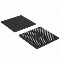
LPC3230FET296,551 NXP Semiconductors, LPC3230FET296,551 Datasheet - Page 3

LPC3230FET296,551
Manufacturer Part Number
LPC3230FET296,551
Description
IC ARM9 MCU 256K 296-TFBGA
Manufacturer
NXP Semiconductors
Series
LPC32x0r
Datasheet
1.OM11079.pdf
(77 pages)
Specifications of LPC3230FET296,551
Core Processor
ARM9
Core Size
16/32-Bit
Speed
266MHz
Connectivity
EBI/EMI, I²C, IrDA, Microwire, SPI, SSI, SSP, UART/USART, USB OTG
Peripherals
DMA, I²S, LCD, Motor Control PWM, PWM, WDT
Number Of I /o
51
Program Memory Type
ROMless
Ram Size
256K x 8
Voltage - Supply (vcc/vdd)
0.9 V ~ 3.6 V
Data Converters
A/D 3x10b
Oscillator Type
Internal
Operating Temperature
-40°C ~ 85°C
Package / Case
296-TFBGA
Processor Series
LPC32
Core
ARM926EJ-S
Data Bus Width
32 bit
Data Ram Size
256 KB
Interface Type
I2C, I2S, UART, USB
Maximum Clock Frequency
20 MHz
Number Of Programmable I/os
51
Number Of Timers
6
Operating Supply Voltage
2.7 V to 3.6 V
Maximum Operating Temperature
+ 85 C
Mounting Style
SMD/SMT
3rd Party Development Tools
MDK-ARM, RL-ARM, ULINK2
Minimum Operating Temperature
- 40 C
On-chip Adc
10 bit, 8 Channel
Lead Free Status / RoHS Status
Lead free / RoHS Compliant
Eeprom Size
-
Program Memory Size
-
Lead Free Status / Rohs Status
Details
Other names
568-4531
935287119551
935287119551
Available stocks
Company
Part Number
Manufacturer
Quantity
Price
Company:
Part Number:
LPC3230FET296,551
Manufacturer:
NXP Semiconductors
Quantity:
10 000
NXP Semiconductors
3. Applications
LPC3220_30_40_50_1
Product data sheet
Standard ARM test/debug interface for compatibility with existing tools.
Emulation Trace Buffer (ETB) with 2048 × 24 bit RAM allows trace via JTAG.
Stop mode saves power while allowing many peripheral functions to restart CPU
activity.
On-chip crystal oscillator.
An on-chip PLL allows CPU operation up to the maximum CPU rate without the
requirement for a high frequency crystal. Another PLL allows operation from the
32 kHz RTC clock rather than the external crystal.
Boundary scan for simplified board testing.
User-accessible unique serial ID number for each chip.
296 pin TFBGA package with a 15 × 15 × 0.7 mm body.
Consumer
Medical
Industrial
Network control
Six enhanced timer/counters which are architecturally identical except for the
peripheral base address. Two capture inputs and two match outputs are pinned out
to four timers. Timer 1 brings out a third match output, timers 2 and 3 bring out all
four match outputs, timer 4 has one match output, and timer 5 has no inputs or
outputs.
32-bit millisecond timer driven from the RTC clock. This timer can generate
interrupts using two match registers.
WatchDog timer clocked by the peripheral clock.
Two single-output PWM blocks.
Motor control PWM.
Keyboard scanner function allows automatic scanning of an up to 8 × 8 key matrix.
Up to 18 external interrupts.
All information provided in this document is subject to legal disclaimers.
Rev. 01.03 — 16 March 2010
LPC3220/30/40/50
16/32-bit ARM microcontrollers
© NXP B.V. 2010. All rights reserved.
3 of 77


