AT91M55800A-33CJ Atmel, AT91M55800A-33CJ Datasheet - Page 213
AT91M55800A-33CJ
Manufacturer Part Number
AT91M55800A-33CJ
Description
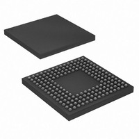
IC ARM MCU 16BIT 176BGA
Manufacturer
Atmel
Series
AT91SAMr
Specifications of AT91M55800A-33CJ
Core Processor
ARM7
Core Size
16/32-Bit
Speed
33MHz
Connectivity
EBI/EMI, SPI, UART/USART
Peripherals
POR, WDT
Number Of I /o
58
Program Memory Type
ROMless
Ram Size
8K x 8
Voltage - Supply (vcc/vdd)
2.7 V ~ 3.6 V
Data Converters
A/D 8x10b; D/A 2x10b
Oscillator Type
Internal
Operating Temperature
-40°C ~ 85°C
Package / Case
176-LFBGA
Processor Series
AT91Mx
Core
ARM7TDMI
Data Bus Width
32 bit
Data Ram Size
8 KB
Interface Type
EBI, SPI, USART
Maximum Clock Frequency
33 MHz
Number Of Programmable I/os
58
Number Of Timers
10 bit
Operating Supply Voltage
3 V to 3.6 V
Maximum Operating Temperature
+ 85 C
Mounting Style
SMD/SMT
3rd Party Development Tools
JTRACE-ARM-2M, MDK-ARM, RL-ARM, ULINK2
Development Tools By Supplier
AT91EB55
Minimum Operating Temperature
- 40 C
On-chip Adc
10 bit, 8 Channel
On-chip Dac
8 bit, 2 Channel
Cpu Family
AT91
Device Core
ARM7TDMI
Device Core Size
32b
Frequency (max)
33MHz
Program Memory Size
Not Required
Total Internal Ram Size
8KB
# I/os (max)
58
Number Of Timers - General Purpose
6
Operating Supply Voltage (typ)
3.3V
Operating Supply Voltage (max)
3.6V
Operating Supply Voltage (min)
2.7V
Instruction Set Architecture
RISC
Operating Temp Range
-40C to 85C
Operating Temperature Classification
Industrial
Mounting
Surface Mount
Pin Count
176
Package Type
BGA
For Use With
AT91EB55 - KIT EVAL FOR ARM AT91M55800A
Lead Free Status / RoHS Status
Contains lead / RoHS non-compliant
Eeprom Size
-
Program Memory Size
-
Lead Free Status / Rohs Status
Lead free / RoHS Compliant
Available stocks
Company
Part Number
Manufacturer
Quantity
Price
Company:

Part Number:
AT91M55800A-33CJ
Manufacturer:
ATMEL
Quantity:
590
Part Number:
AT91M55800A-33CJ
Manufacturer:
ATMEL/爱特梅尔
Quantity:
20 000
Company:
Part Number:
AT91M55800A-33CJ SL383
Manufacturer:
Atmel
Quantity:
10 000


21.0.1
21.0.2
21.0.3
21.0.4
1745F–ATARM–06-Sep-07
Analog-to-digital Conversion
Conversion Results
Conversion Triggers
Sleep Mode
The ADC has an internal sample-and-hold circuit that holds the sampled analog value during a
complete conversion.
The reference voltage pin ADVREF allows the analog input conversion range to be set between
0 and ADVREF. Analog inputs between these voltages convert to values based on a linear
conversion.
The ADC uses the ADC Clock to perform the conversion. To convert a single analog value to a
10-bit digital data requires 11 ADC clock cycles. The ADC Clock frequency is selected in the
PRESCAL field of the Mode Register (ADC_MR).
When a conversion is complete, the resulting 10-bit digital value is stored in the Convert Data
Register (ADC_CDR) of the selected channel, and the corresponding EOC flag in the Status
Register (ADC_SR) is set. This bit can provide an interrupt signal and is automatically cleared
when the corresponding Convert Data Register (ADC_CDR) is read.
If the ADC_CDR is not read before further incoming data is converted, the corresponding Over-
run Error (OVRE) flag is set in the Status Register (ADC_SR).
The ADC offers an 8-bit or 10-bit operating mode. By default after a reset, the ADC operates in
10-bit mode. If the bit RES in ADC_MR is set, the 8-bit mode is selected.
When operating in 10-bit mode, the field DATA in ADC_CDR is fully significant.
When operating in 8-bit mode, only the 8 lowest bits of DATA are significant and the 2 highest
bits read 0.
Conversions of the active analog channels are started with a software or a hardware trigger. The
software trigger is provided by writing the bit START in the Control Register (ADC_CR).
The hardware trigger can be one of the TIOA outputs of the Timer Counter channels, or the
external trigger input of the ADC (AD0TRIG for the ADC0 or AD1TRIG for ADC1). The hardware
trigger is selected with the field TRGSEL in the Mode Register (ADC_MR). The selected hard-
ware trigger is enabled with the bit TRGEN in the Mode Register (ADC_MR).
If a hardware trigger is selected, the start of a conversion is detected at each rising edge of the
selected signal. If one of the TIOA outputs is selected, the corresponding Timer Counter channel
must be programmed in Waveform Mode.
Only one start command is necessary to initiate a conversion sequence on all the channels. The
ADC hardware logic automatically performs the conversions on the active channels, then waits
for a new request. The Channel Enable (ADC_CHER) and Channel Disable (ADC_CHDR) Reg-
isters enable the analog channels to be enabled or disabled independently.
The AT91 ADC Sleep Mode maximizes power saving by deactivating the ADC when it is not
being used for conversions. Sleep Mode is selected by setting the bit SLEEP in the Mode Regis-
ter ADC_MR.
When a start conversion request occurs, the ADC is automatically activated. As the analog cell
requires a start-up time, the logic waits during this time and starts the conversion sequence on
AT91M5880A
213
Related parts for AT91M55800A-33CJ
Image
Part Number
Description
Manufacturer
Datasheet
Request
R

Part Number:
Description:
IC ARM7 MCU 176 TQFP
Manufacturer:
Atmel
Datasheet:

Part Number:
Description:
IC ARM7 MCU 176 BGA
Manufacturer:
Atmel
Datasheet:

Part Number:
Description:
DEV KIT FOR AVR/AVR32
Manufacturer:
Atmel
Datasheet:

Part Number:
Description:
INTERVAL AND WIPE/WASH WIPER CONTROL IC WITH DELAY
Manufacturer:
ATMEL Corporation
Datasheet:
Part Number:
Description:
Low-Voltage Voice-Switched IC for Hands-Free Operation
Manufacturer:
ATMEL Corporation
Datasheet:
Part Number:
Description:
MONOLITHIC INTEGRATED FEATUREPHONE CIRCUIT
Manufacturer:
ATMEL Corporation
Datasheet:
Part Number:
Description:
AM-FM Receiver IC U4255BM-M
Manufacturer:
ATMEL Corporation
Datasheet:
Part Number:
Description:
Monolithic Integrated Feature Phone Circuit
Manufacturer:
ATMEL Corporation
Datasheet:
Part Number:
Description:
Multistandard Video-IF and Quasi Parallel Sound Processing
Manufacturer:
ATMEL Corporation
Datasheet:
Part Number:
Description:
High-performance EE PLD
Manufacturer:
ATMEL Corporation
Datasheet:
Part Number:
Description:
8-bit Flash Microcontroller
Manufacturer:
ATMEL Corporation
Datasheet:
Part Number:
Description:
2-Wire Serial EEPROM
Manufacturer:
ATMEL Corporation
Datasheet: