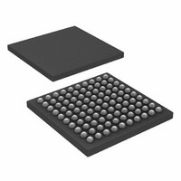
ATSAM3S4CA-CU Atmel, ATSAM3S4CA-CU Datasheet - Page 861

ATSAM3S4CA-CU
Manufacturer Part Number
ATSAM3S4CA-CU
Description
IC MCU 32BIT 256KB FLASH 100BGA
Manufacturer
Atmel
Series
SAM3Sr
Specifications of ATSAM3S4CA-CU
Core Processor
ARM® Cortex-M3™
Core Size
32-Bit
Speed
64MHz
Connectivity
EBI/EMI, I²C, MMC, SPI, SSC, UART/USART, USB
Peripherals
Brown-out Detect/Reset, DMA, I²S, POR, PWM, WDT
Number Of I /o
79
Program Memory Size
256KB (256K x 8)
Program Memory Type
FLASH
Ram Size
48K x 8
Voltage - Supply (vcc/vdd)
1.62 V ~ 1.95 V
Data Converters
A/D 16x10/12b, D/A 2x12b
Oscillator Type
Internal
Operating Temperature
-40°C ~ 85°C
Package / Case
100-LFBGA
Processor Series
ATSAM3x
Core
ARM Cortex M3
3rd Party Development Tools
JTRACE-CM3, MDK-ARM, RL-ARM, ULINK2
Development Tools By Supplier
ATSAM3S-EK
Package
100LFBGA
Device Core
ARM Cortex M3
Family Name
AT91
Maximum Speed
64 MHz
Operating Supply Voltage
1.8|3.3 V
Data Bus Width
32 Bit
Number Of Programmable I/os
79
Interface Type
I2C/I2S/SPI/UART/USART/USB
On-chip Adc
16-chx12-bit
On-chip Dac
2-chx12-bit
Number Of Timers
6
Lead Free Status / RoHS Status
Lead free / RoHS Compliant
Eeprom Size
-
Lead Free Status / Rohs Status
Details
Available stocks
Company
Part Number
Manufacturer
Quantity
Price
Company:
Part Number:
ATSAM3S4CA-CU
Manufacturer:
SANYO
Quantity:
1 000
- Current page: 861 of 1118
- Download datasheet (24Mb)
Figure 36-10. Method 1 (UPDM = 0)
6500C–ATARM–8-Feb-11
Method 1: Manual write of duty-cycle values and manual trigger of the update
UPDULOCK
CDTYUPD
CCNT0
CDTY
0x20
0x20
In this mode, the update of the period value, the duty-cycle values and the dead-time values
must be done by writing in their respective update registers with the CPU (respectively
PWM_CPRDUPDx, PWM_CDTYUPDx and PWM_DTUPDx).
To trigger the update, the user must use the bit UPDULOCK of the
Update Control Register”
PWM period) the synchronous channels:
After writing the UPDULOCK bit to 1, it is held at this value until the update occurs, then it is read
0.
Sequence for Method 1:
• If the bit UPDULOCK is set to 1, the update is done at the next PWM period of the
• If the UPDULOCK bit is not set to 1, the update is locked and cannot be performed.
1. Select the manual write of duty-cycle values and the manual update by setting the
2. Define the synchronous channels by the SYNCx bits in the PWM_SCM register.
3. Enable the synchronous channels by writing CHID0 in the PWM_ENA register.
4. If an update of the period value and/or the duty-cycle values and/or the dead-time val-
5. Set UPDULOCK to 1 in PWM_SCUC.
6. The update of the registers will occur at the beginning of the next PWM period. At this
synchronous channels.
UPDM field to 0 in the PWM_SCM register
ues is required, write registers that need to be updated (PWM_CPRDUPDx,
PWM_CDTYUPDx and PWM_DTUPDx).
moment the UPDULOCK bit is reset, go to
0x40
0x40
0x60
(PWM_SCUC) which allows to update synchronously (at the same
0x60
Step
4.) for new values.
SAM3S Preliminary
“PWM Sync Channels
861
Related parts for ATSAM3S4CA-CU
Image
Part Number
Description
Manufacturer
Datasheet
Request
R

Part Number:
Description:
KIT EVAL FOR ATSAM3S4C
Manufacturer:
Atmel
Datasheet:

Part Number:
Description:
Development Boards & Kits - ARM EVAL KIT SAM3S8 & SAM3SD8 series
Manufacturer:
Atmel
Datasheet:

Part Number:
Description:
AT91 ARM Cortex M3-based Processor
Manufacturer:
ATMEL [ATMEL Corporation]
Datasheet:

Part Number:
Description:
DEV KIT FOR AVR/AVR32
Manufacturer:
Atmel
Datasheet:

Part Number:
Description:
INTERVAL AND WIPE/WASH WIPER CONTROL IC WITH DELAY
Manufacturer:
ATMEL Corporation
Datasheet:

Part Number:
Description:
Low-Voltage Voice-Switched IC for Hands-Free Operation
Manufacturer:
ATMEL Corporation
Datasheet:

Part Number:
Description:
MONOLITHIC INTEGRATED FEATUREPHONE CIRCUIT
Manufacturer:
ATMEL Corporation
Datasheet:

Part Number:
Description:
AM-FM Receiver IC U4255BM-M
Manufacturer:
ATMEL Corporation
Datasheet:

Part Number:
Description:
Monolithic Integrated Feature Phone Circuit
Manufacturer:
ATMEL Corporation
Datasheet:

Part Number:
Description:
Multistandard Video-IF and Quasi Parallel Sound Processing
Manufacturer:
ATMEL Corporation
Datasheet:

Part Number:
Description:
High-performance EE PLD
Manufacturer:
ATMEL Corporation
Datasheet:

Part Number:
Description:
8-bit Flash Microcontroller
Manufacturer:
ATMEL Corporation
Datasheet:


