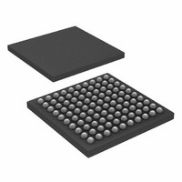
ATSAM3S4CA-CU Atmel, ATSAM3S4CA-CU Datasheet - Page 989

ATSAM3S4CA-CU
Manufacturer Part Number
ATSAM3S4CA-CU
Description
IC MCU 32BIT 256KB FLASH 100BGA
Manufacturer
Atmel
Series
SAM3Sr
Specifications of ATSAM3S4CA-CU
Core Processor
ARM® Cortex-M3™
Core Size
32-Bit
Speed
64MHz
Connectivity
EBI/EMI, I²C, MMC, SPI, SSC, UART/USART, USB
Peripherals
Brown-out Detect/Reset, DMA, I²S, POR, PWM, WDT
Number Of I /o
79
Program Memory Size
256KB (256K x 8)
Program Memory Type
FLASH
Ram Size
48K x 8
Voltage - Supply (vcc/vdd)
1.62 V ~ 1.95 V
Data Converters
A/D 16x10/12b, D/A 2x12b
Oscillator Type
Internal
Operating Temperature
-40°C ~ 85°C
Package / Case
100-LFBGA
Processor Series
ATSAM3x
Core
ARM Cortex M3
3rd Party Development Tools
JTRACE-CM3, MDK-ARM, RL-ARM, ULINK2
Development Tools By Supplier
ATSAM3S-EK
Package
100LFBGA
Device Core
ARM Cortex M3
Family Name
AT91
Maximum Speed
64 MHz
Operating Supply Voltage
1.8|3.3 V
Data Bus Width
32 Bit
Number Of Programmable I/os
79
Interface Type
I2C/I2S/SPI/UART/USART/USB
On-chip Adc
16-chx12-bit
On-chip Dac
2-chx12-bit
Number Of Timers
6
Lead Free Status / RoHS Status
Lead free / RoHS Compliant
Eeprom Size
-
Lead Free Status / Rohs Status
Details
Available stocks
Company
Part Number
Manufacturer
Quantity
Price
Company:
Part Number:
ATSAM3S4CA-CU
Manufacturer:
SANYO
Quantity:
1 000
- Current page: 989 of 1118
- Download datasheet (24Mb)
39.6.11
6500C–ATARM–8-Feb-11
6500C–ATARM–8-Feb-11
PDC Buffer Structure
A minimal Tracking Time is necessary for the ADC to guarantee the best converted final value
between two channel selections. This time has to be programmed through the TRACKTIM bit
field in the Mode Register, ADC_MR.
When the gain, offset or differential input parameters of the analog cell change between two
channels, the analog cell may need a specific settling time before starting the tracking phase. In
that case, the controller automatically waits during the settling time defined in the
Register”. Obviously, if the ANACH option is not set, this time is unused.
Warning: No input buffer amplifier to isolate the source is included in the ADC. This must be
taken into consideration to program a precise value in the TRACKTIM field. See the product
ADC Characteristics section.
The PDC read channel is triggered each time a new data is stored in ADC_LCDR register. The
same structure of data is repeatedly stored in ADC_LCDR register each time a trigger event
occurs. Depending on user mode of operation (ADC_MR, ADC_CHSR, ADC_SEQR1,
ADC_SEQR2) the structure differs. Each data transferred to PDC buffer, carried on a half-word
(16-bit), consists of last converted data right aligned and when TAG is set in ADC_EMR register,
the 4 most significant bits are carrying the channel number thus allowing an easier post-process-
ing in the PDC buffer or better checking the PDC buffer integrity.
SAM3S Preliminary
SAM3S Preliminary
“ADC Mode
989
989
Related parts for ATSAM3S4CA-CU
Image
Part Number
Description
Manufacturer
Datasheet
Request
R

Part Number:
Description:
KIT EVAL FOR ATSAM3S4C
Manufacturer:
Atmel
Datasheet:

Part Number:
Description:
Development Boards & Kits - ARM EVAL KIT SAM3S8 & SAM3SD8 series
Manufacturer:
Atmel
Datasheet:

Part Number:
Description:
AT91 ARM Cortex M3-based Processor
Manufacturer:
ATMEL [ATMEL Corporation]
Datasheet:

Part Number:
Description:
DEV KIT FOR AVR/AVR32
Manufacturer:
Atmel
Datasheet:

Part Number:
Description:
INTERVAL AND WIPE/WASH WIPER CONTROL IC WITH DELAY
Manufacturer:
ATMEL Corporation
Datasheet:

Part Number:
Description:
Low-Voltage Voice-Switched IC for Hands-Free Operation
Manufacturer:
ATMEL Corporation
Datasheet:

Part Number:
Description:
MONOLITHIC INTEGRATED FEATUREPHONE CIRCUIT
Manufacturer:
ATMEL Corporation
Datasheet:

Part Number:
Description:
AM-FM Receiver IC U4255BM-M
Manufacturer:
ATMEL Corporation
Datasheet:

Part Number:
Description:
Monolithic Integrated Feature Phone Circuit
Manufacturer:
ATMEL Corporation
Datasheet:

Part Number:
Description:
Multistandard Video-IF and Quasi Parallel Sound Processing
Manufacturer:
ATMEL Corporation
Datasheet:

Part Number:
Description:
High-performance EE PLD
Manufacturer:
ATMEL Corporation
Datasheet:

Part Number:
Description:
8-bit Flash Microcontroller
Manufacturer:
ATMEL Corporation
Datasheet:


