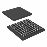
ATSAM3S4CA-CU Atmel, ATSAM3S4CA-CU Datasheet - Page 956

ATSAM3S4CA-CU
Manufacturer Part Number
ATSAM3S4CA-CU
Description
IC MCU 32BIT 256KB FLASH 100BGA
Manufacturer
Atmel
Series
SAM3Sr
Specifications of ATSAM3S4CA-CU
Core Processor
ARM® Cortex-M3™
Core Size
32-Bit
Speed
64MHz
Connectivity
EBI/EMI, I²C, MMC, SPI, SSC, UART/USART, USB
Peripherals
Brown-out Detect/Reset, DMA, I²S, POR, PWM, WDT
Number Of I /o
79
Program Memory Size
256KB (256K x 8)
Program Memory Type
FLASH
Ram Size
48K x 8
Voltage - Supply (vcc/vdd)
1.62 V ~ 1.95 V
Data Converters
A/D 16x10/12b, D/A 2x12b
Oscillator Type
Internal
Operating Temperature
-40°C ~ 85°C
Package / Case
100-LFBGA
Processor Series
ATSAM3x
Core
ARM Cortex M3
3rd Party Development Tools
JTRACE-CM3, MDK-ARM, RL-ARM, ULINK2
Development Tools By Supplier
ATSAM3S-EK
Package
100LFBGA
Device Core
ARM Cortex M3
Family Name
AT91
Maximum Speed
64 MHz
Operating Supply Voltage
1.8|3.3 V
Data Bus Width
32 Bit
Number Of Programmable I/os
79
Interface Type
I2C/I2S/SPI/UART/USART/USB
On-chip Adc
16-chx12-bit
On-chip Dac
2-chx12-bit
Number Of Timers
6
Lead Free Status / RoHS Status
Lead free / RoHS Compliant
Eeprom Size
-
Lead Free Status / Rohs Status
Details
Available stocks
Company
Part Number
Manufacturer
Quantity
Price
Company:
Part Number:
ATSAM3S4CA-CU
Manufacturer:
SANYO
Quantity:
1 000
- Current page: 956 of 1118
- Download datasheet (24Mb)
• TXCOMP: Generates an IN Packet with Data Previously Written in the DPR
This flag generates an interrupt while it is set to one.
Write (Cleared by the firmware):
0 = Clear the flag, clear the interrupt.
1 = No effect.
Read (Set by the USB peripheral):
0 = Data IN transaction has not been acknowledged by the Host.
1 = Data IN transaction is achieved, acknowledged by the Host.
After having issued a Data IN transaction setting TXPKTRDY, the device firmware waits for TXCOMP to be sure that the
host has acknowledged the transaction.
• RX_DATA_BK0: Receive Data Bank 0
This flag generates an interrupt while it is set to one.
Write (Cleared by the firmware):
0 = Notify USB peripheral device that data have been read in the FIFO's Bank 0.
1 = To leave the read value unchanged.
Read (Set by the USB peripheral):
0 = No data packet has been received in the FIFO's Bank 0.
1 = A data packet has been received, it has been stored in the FIFO's Bank 0.
When the device firmware has polled this bit or has been interrupted by this signal, it must transfer data from the FIFO to
the microcontroller memory. The number of bytes received is available in RXBYTCENT field. Bank 0 FIFO values are read
through the UDP_FDRx register. Once a transfer is done, the device firmware must release Bank 0 to the USB peripheral
device by clearing RX_DATA_BK0.
956
/// Clears the specified bit(s) in the UDP_CSR register.
/// \param endpoint The endpoint number of the CSR to process.
/// \param flags The bitmap to clear to 0.
#define CLEAR_CSR(endpoint, flags) \
for( nop_count=0; nop_count<15; nop_count++ ) {\
In a preemptive environment, set or clear the flag and wait for a time of 1 UDPCK clock cycle and
1peripheral clock cycle. However, RX_DATA_BK0, TXPKTRDY, RX_DATA_BK1 require wait times of 3 UDPCK
clock cycles and 5 peripheral clock cycles before accessing DPR.
{ \
}
}
SAM3S Preliminary
volatile unsigned int reg; \
reg = AT91C_BASE_UDP->UDP_CSR[endpoint]; \
reg |= REG_NO_EFFECT_1_ALL; \
reg &= ~(flags); \
AT91C_BASE_UDP->UDP_CSR[endpoint] = reg; \
}\
nop();\
6500C–ATARM–8-Feb-11
Related parts for ATSAM3S4CA-CU
Image
Part Number
Description
Manufacturer
Datasheet
Request
R

Part Number:
Description:
KIT EVAL FOR ATSAM3S4C
Manufacturer:
Atmel
Datasheet:

Part Number:
Description:
Development Boards & Kits - ARM EVAL KIT SAM3S8 & SAM3SD8 series
Manufacturer:
Atmel
Datasheet:

Part Number:
Description:
AT91 ARM Cortex M3-based Processor
Manufacturer:
ATMEL [ATMEL Corporation]
Datasheet:

Part Number:
Description:
DEV KIT FOR AVR/AVR32
Manufacturer:
Atmel
Datasheet:

Part Number:
Description:
INTERVAL AND WIPE/WASH WIPER CONTROL IC WITH DELAY
Manufacturer:
ATMEL Corporation
Datasheet:

Part Number:
Description:
Low-Voltage Voice-Switched IC for Hands-Free Operation
Manufacturer:
ATMEL Corporation
Datasheet:

Part Number:
Description:
MONOLITHIC INTEGRATED FEATUREPHONE CIRCUIT
Manufacturer:
ATMEL Corporation
Datasheet:

Part Number:
Description:
AM-FM Receiver IC U4255BM-M
Manufacturer:
ATMEL Corporation
Datasheet:

Part Number:
Description:
Monolithic Integrated Feature Phone Circuit
Manufacturer:
ATMEL Corporation
Datasheet:

Part Number:
Description:
Multistandard Video-IF and Quasi Parallel Sound Processing
Manufacturer:
ATMEL Corporation
Datasheet:

Part Number:
Description:
High-performance EE PLD
Manufacturer:
ATMEL Corporation
Datasheet:

Part Number:
Description:
8-bit Flash Microcontroller
Manufacturer:
ATMEL Corporation
Datasheet:


